ADS1115 HAL modul I2c communication
- fupeama
-
 Topic Author
- Offline
- Senior Member
-

Less
More
- Posts: 73
- Thank you received: 16
11 Jun 2015 20:48 - 11 Jun 2015 20:58 #59706
by fupeama
ADS1115 HAL modul I2c communication was created by fupeama
Hi,
I upgraded my old HX711 modul.
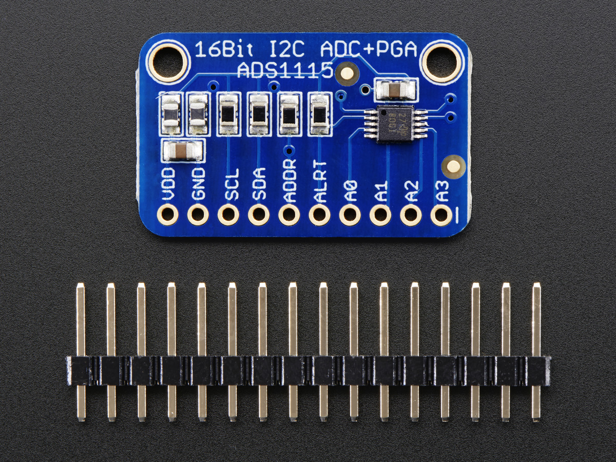
Now I used another one adc converter. ADS1115. 4x single-ended or 2xdifferential inputs.
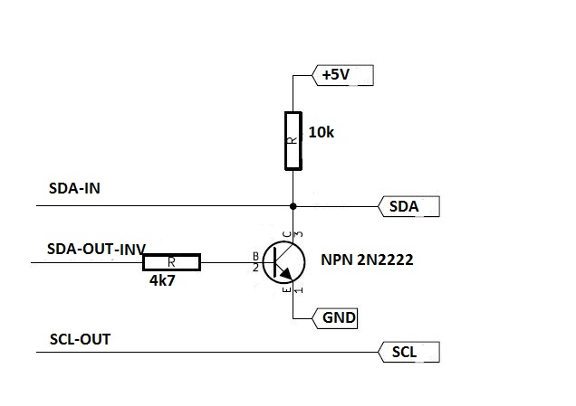
It is possible to used it with parport (2x out pins 1x in pin)
two resistors and one NPN transistor are needed.
All files are included in zip file. ads1115.hal and config file for parport
Martin
I upgraded my old HX711 modul.
Now I used another one adc converter. ADS1115. 4x single-ended or 2xdifferential inputs.
It is possible to used it with parport (2x out pins 1x in pin)
two resistors and one NPN transistor are needed.
All files are included in zip file. ads1115.hal and config file for parport
Martin
Last edit: 11 Jun 2015 20:58 by fupeama.
The following user(s) said Thank You: mehdidadash
Please Log in or Create an account to join the conversation.
- fupeama
-
Topic Author
- Offline
- Senior Member
-
Less
More
- Posts: 73
- Thank you received: 16
15 Jun 2015 18:53 #59840
by fupeama
Replied by fupeama on topic ADS1115 HAL modul I2c communication
Hi,
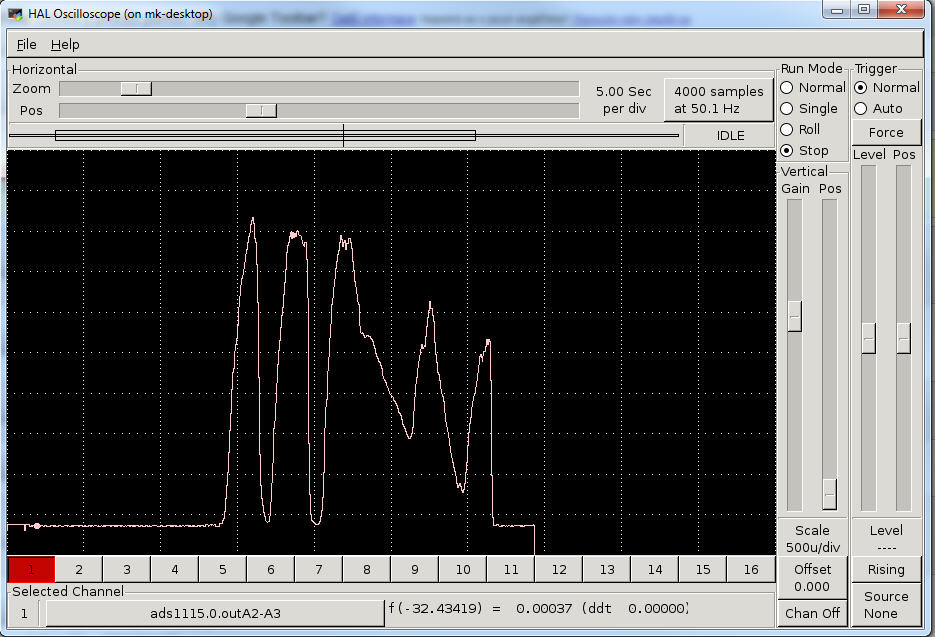
I change output value from raw (0-32767) to +-volts depends on GAIN sets up on [11:9] bits in MSB parrametr.
I tried connect load cell dirrect to ads1115 without any amplifier, and result is good for my purpose. There is 10bits resolutin.
Modul update value every 10ms/channel. It means every 40ms for all 4 configured channels.
I want use this modul in my different project like feadback spindle speed from VFD.
0-10V VFD ->convert 0-5V -> ads1115 -> linuxcnc
Martin
M
I change output value from raw (0-32767) to +-volts depends on GAIN sets up on [11:9] bits in MSB parrametr.
I tried connect load cell dirrect to ads1115 without any amplifier, and result is good for my purpose. There is 10bits resolutin.
Modul update value every 10ms/channel. It means every 40ms for all 4 configured channels.
I want use this modul in my different project like feadback spindle speed from VFD.
0-10V VFD ->convert 0-5V -> ads1115 -> linuxcnc
Martin
// This is a component for EMC2 HAL
// Copyright 2015 Martin Kaplan <fupeama@gmail.com>
//
// This program is free software; you can redistribute it and/or modify
// it under the terms of the GNU General Public License as published by
// the Free Software Foundation; either version 2 of the License, or
// (at your option) any later version.
//
// This program is distributed in the hope that it will be useful,
// but WITHOUT ANY WARRANTY; without even the implied warranty of
// MERCHANTABILITY or FITNESS FOR A PARTICULAR PURPOSE. See the
// GNU General Public License for more details.
//
// You should have received a copy of the GNU General Public License
// along with this program; if not, write to the Free Software
// Foundation, Inc., 59 Temple Place, Suite 330, Boston, MA 02111-1307 USA
component ads1115 "I2C Interface for ADC ADS1115 (ADS1113 and ADS1114)";
description """
This component is designed as an interface between ADC analog-digital-converter ADS1115 16bit and LINUXCNC through I2C protocol
.SH SYNOPSIS
(ignore the auto-generated SYNOPSIS above)
.SH
.HP
.B loadrt ads1115 cfg=ssd,dd\\fB
Means load two component ads1115. First with two single-ended inputs on pins A0 A1 and one differential input on pins A2 A3.
Second with two differetial inputs on A0 A1 and A2 A3.
Each instance of the component is defined by a group of letters describing the
type of analog inputs. A comma separates individual instances of the component.
.SH Tags
Input type definitions are all lower-case.
s=single-ended (used one pin on ads1115)
d=differencial (used two pins on ads1115)
ADS1115 has 4 input pins A0-A3
The ADS1115 operate from a single power supply VOLTAGE REFERENCE ranging from 2.0V to 5.5V.
An onboard PGA is available on the ADS1114 and ADS1115 that offers input ranges from the supply to as low as ±256mV, allowing both large and small signals to be measured with high resolution.
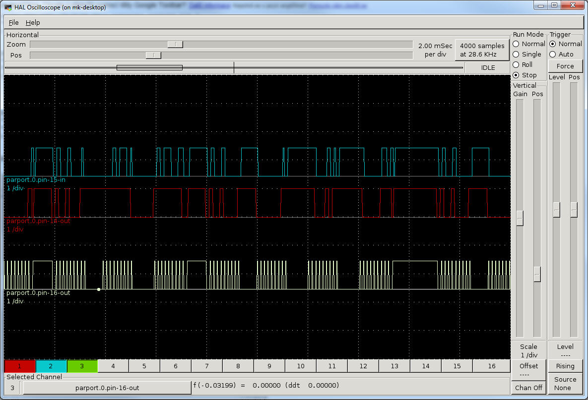
The ADS1115 communicate with the master (LINUXCNC) through an I2C interface. The master provides a clock signal on the SCL pin and data are transferred via the SDA pin.
.B QUICKSTART GUIDE
Modul automacally generated appropriated pins and parameters for ADS based on cfg sequence.
Communication with ads1115 repeats in cycles:A
Select input (A0-A3)
Send i2c address folowed by write bit to ADC
Send Pointer register for write to Config register (BIT1=0 BIT0=1)
Send MSB Byte (default value are generated by cfg string)
Send LSB Byte
Send address folowed by write bit to ADC
Send Pointer register for read Conversion register (BIT1=0 BIT0=0)
Send i2c address followed by read bit
Read MSB
Read LSB
Go to start with next input
For example to set up gain amplifier to 4.096V (default value = 2.048V) on single-ended input on A0 change A0msb parameter from default value 0xc5 to 0xc3.
0xc5 1100 0101 bit[15]=1 bits[14:12]=100 bits[11:9]=010 bit[8]=1
0xc3 1100 0011 bit[15]=1 bits[14:12]=100 bits[11:9]=001 bit[8]=1
See Config Register
.B REGISTERS
The ADS1115 have four registers that are accessible via the I2C port. The Conversion register contains the result of the last conversion. The Config register allows the user to change the ADS1115 operating modes and query the status of the devices. Two registers, Lo_thresh and Hi_thresh, set the threshold values used for the comparator function.
.B POINTER REGISTER
The four registers are accessed by writing to the Pointer register byte.
BIT 1 BIT 0 REGISTER
0 0 Conversion register
0 1 Config register
1 0 LO_Treshold register
1 1 HI_Treshold register
.B CONVERSION REGISTER
The 16-bit register contains the result of the last conversion in binary twos complement format.
.B CONFIG REGISTER
The 16-bit register can be used to control the ADS1115 operating mode, input selection, data rate, PGA settings, and comparator modes.
Pointer Register Byte (Write-Only)
BIT_7 BIT_6 BIT_5 BIT_4 BIT_3 BIT_2 BIT_1 BIT_0
0 0 0 0 0 0 Reg address
Conversion Register (Read-Only)
BIT 15 14 13 12 11 10 9 8 7 6 5 4 3 2 1 0
NAME D15 D14 D13 D12 D11 D10 D9 D8 D7 D6 D5 D4 D3 D2 D1 D0
Config Register (Read/Write)
MSB
BIT 15 14 13 12 11 10 9 8
NAME OS MUX2 MUX1 MUX0 PGA2 PGA1 PGA0 MODE
LSB
BIT 7 6 5 4 3 2 1 0
NAME DR2 DR1 DR0 COMP_MODE COMP_POL COMP_LAT COMP_QUE1 COMP_QUE0
.B Bit[15] OS: Operation Status
For a write status:
0 : No effect
1 : Begin a single conversion (when in power-down mode)
For a read status:
0 : Device is currently performing a conversion
1 : Device is not currently performing a conversion
.B Bits [14:12] MUX[2:0]: Input multiplexer configuration
These bits configure the input multiplexer.
000 : AINP = AIN0 and AINN = AIN1 100 : AINP = AIN0 and AINN = GND
001 : AINP = AIN0 and AINN = AIN3 101 : AINP = AIN1 and AINN = GND
010 : AINP = AIN1 and AINN = AIN3 110 : AINP = AIN2 and AINN = GND
011 : AINP = AIN2 and AINN = AIN3 111 : AINP = AIN3 and AINN = GND
.B Bits [11:9] PGA[2:0]: Programmable gain amplifier configuration
These bits configure the programmable gain amplifier. They serve no function on the ADS1113.
000 : FS = ±6.144V(1) 100 : FS = ±0.512V
001 : FS = ±4.096V(1) 101 : FS = ±0.256V
010 : FS = ±2.048V (default) 110 : FS = ±0.256V
011 : FS = ±1.024V 111 : FS = ±0.256V
.B Bit [8] MODE: Device operating mode
This bit controls the current operational mode
0 : Continuous conversion mode
1 : Power-down single-shot mode (default)
.B Bits [7:5] DR[2:0]: Data rate
These bits control the data rate setting.
000 : 8SPS 100 : 128SPS (default)
001 : 16SPS 101 : 250SPS
010 : 32SPS 110 : 475SPS
011 : 64SPS 111 : 860SPS
.B Bit [4] COMP_MODE: Comparator mode
This bit controls the comparator mode of operation. It changes whether the comparator is implemented as a
traditional comparator (COMP_MODE = '0') or as a window comparator (COMP_MODE = '1').
0 : Traditional comparator with hysteresis (default)
1 : Window comparator
.B Bit [3] COMP_POL: Comparator polarity
This bit controls the polarity of the ALERT/RDY pin. When COMP_POL = '0' the comparator output is active
low. When COMP_POL='1' the ALERT/RDY pin is active high.
0 : Active low (default)
1 : Active high
.B Bit [2] COMP_LAT: Latching comparator
This bit controls whether the ALERT/RDY pin latches once asserted or clears once conversions are within the
margin of the upper and lower threshold values. When COMP_LAT = '0', the ALERT/RDY pin does not latch
when asserted. When COMP_LAT = '1', the asserted ALERT/RDY pin remains latched until conversion data
are read by the master or an appropriate SMBus alert response is sent by the master, the device responds with
its address, and it is the lowest address currently asserting the ALERT/RDY bus line.
0 : Non-latching comparator (default)
1 : Latching comparator
.B Bits [1:0] COMP_QUE: Comparator queue and disable
These bits perform two functions. When set to '11', they disable the comparator function and put the
ALERT/RDY pin into a high state. When set to any other value, they control the number of successive
conversions exceeding the upper or lower thresholds required before asserting the ALERT/RDY pin.
00 : Assert after one conversion
01 : Assert after two conversions
10 : Assert after four conversions
11 : Disable comparator (default)
.B Lo_thresh AND Hi_thresh REGISTERS
Set up tresholds registers are not inplemented on this modul.
""";
pin in bit SDAIn "SDA Input pin";
pin out bit SDAOut "SDA Output pin";
pin out bit SCLOut "SCL Output pin";
pin in bit enable=1 "Turn communication on or offi (default=on)";
pin out bit communication"Communication is ok. True when ADC send Acknowledge bits";
pin out float outA0 if (personality & 0x01)"Analog value between A0 single-ended and GND pins";
pin out float outA1 if (personality & 0x02)"Analog value between A1 single-ended and GND pins";
pin out float outA0-A1 if (personality & 0x04)"Analog value between A0 and A1 pins";
pin out float outA2 if (personality & 0x08)"Analog value between A2 single-ended and GND pins";
pin out float outA3 if (personality & 0x10)"Analog value between A3 single-ended and GND pins";
pin out float outA2-A3 if (personality & 0x20)"Analog value between A2 and A3 pins";
param rw unsigned A0msb=0xc5 if (personality & 0x01) "MSB byte for A0";
param rw unsigned A0lsb=0x83 if (personality & 0x01) "LSB byte for A0";
param rw unsigned A1msb=0xd5 if (personality & 0x02) "MSB byte for A1";
param rw unsigned A1lsb=0x83 if (personality & 0x02) "LSB byte for A1";
param rw unsigned A0-A1msb=0x85 if (personality & 0x04)"MSB byte for A0-A1";
param rw unsigned A0-A1lsb=0x83 if (personality & 0x04)"LSB byte for A0-A1";
param rw unsigned A2msb=0xe5 if (personality & 0x08) "MSB byte for A2";
param rw unsigned A2lsb=0x83 if (personality & 0x08) "LSB byte for A2";
param rw unsigned A3msb=0xf5 if (personality & 0x10) "MSB byte for A3";
param rw unsigned A3lsb=0x83 if (personality & 0x10) "LSB byte for A3";
param rw unsigned A2-A3msb=0xb5 if (personality & 0x20)"MSB byte for A2-A3";
param rw unsigned A2-A3lsb=0x83 if (personality & 0x20)"LSB byte for A2-A3";
param rw unsigned address = 0x48 "address selector-ADDR PIN 0x48=GROUND,0x49=VDD";
function make_puls nofp "Fast thread for generating puls";
function read fp "Slow thread for read value from ADC";
option extra_setup yes;
option count_function yes;
option personality;
license "GPL";
author "Martin Kaplan";
variable u32 ACKcount=0;
variable int ByteStatus = 0;
variable int BitStatus = 0;
variable int ByteNum = 8;
variable u16 TXByte;
variable u16 TXBit;
variable u16 RXByte;
variable u16 RXBit;
variable u16 RxWord [10];
variable int wordnum =0;
variable int lastwordnum;
variable int sentense=0;
variable int lastsentense;
variable int CmdByte = 0;
variable int RxByteNum = 0;
variable u32 wait;
variable double timer;
variable float fs;
;;
enum I2C_mask
{
StartBit = 0x0100, //Generate SDA High>Low on SCL is High
AckBit = 0x0200, //Send low on SDA if Dir=Read
StopBit = 0x0400, //Genarate SDA Low>High on SCL is High
DirBit = 0x0800, // Direction 0=write 1=read
WaitBit = 0x1000, //Wait for ms on 0xffff position
AddressBit = 0x2000, //Write address to byte
ParamMSBBit = 0x4000, //mask byte by parameter MSB
ParamLSBBit = 0x8000 //mask byte by parameter LSB
};
enum I2C_Byte_status
{
ByteIdle = 0, //Idle
ByteNew = 1, //New byte
ByteStart = 2, //Start byte
Byte7_1 = 3, //Bytes 1-7
Byte0 = 4, //Last Byte
ByteAck = 5, //ACK
ByteStop = 6 //Stop byte
};
enum I2C_Bit_Status
{
BitIdle = 0, //Bit is IDLE
BitNew = 1, //Send TXbit to SDA
BitData = 2, //Send High to SCL
BitLow = 3, //SCL is Low
BitHigh = 4, //SCL is Hig
BitStart = 5, //Send SDA High->Low while SCL is High
BitStop = 6 //Send SDA Lowi->High while SCL is High
};
#define MAX_CHAN 4
#define MAX_TXWORDS 10
const u16 TXWord[MAX_TXWORDS] = {0x2100, 0x01, 0x4000, 0x8400, 0x1002, 0x2100, 0x400, 0x2101, 0xa00, 0xe00};
const float GAIN[] = {6.144, 4.096, 2.048, 1.024, 0.512, 0.256, 0.256, 0.256};
static char *cfg[MAX_CHAN];
RTAPI_MP_ARRAY_STRING(cfg, MAX_CHAN, "Description of each channel");
FUNCTION(make_puls)
{
if (enable) {
// Cycles through Bytes
if (BitStatus == BitIdle){
switch (ByteStatus) {
case ByteNew :
if ((TXByte & StartBit) == StartBit){
ByteStatus=ByteStart;
TXBit = 1;
BitStatus = BitNew;
} else {
ByteStatus=Byte7_1;
}
break;
case ByteStart :
ByteStatus = Byte7_1;
break;
case Byte7_1 :
ByteNum--;
TXBit = ((TXByte & DirBit)==0) ? (TXByte >> ByteNum) & 0x01 : 1;
RXByte = (RXByte << 1) | RXBit;
if (ByteNum == 0){
ByteNum=8;
ByteStatus=Byte0;
}
BitStatus = BitNew;
break;
case Byte0 :
TXBit=((TXByte & DirBit)==0) ? 1 : ((TXByte>>9) & 0x01) ^0x01; //ACK
RXByte = (RXByte << 1) | RXBit;
BitStatus = BitNew;
ByteStatus = ByteAck;
break;
case ByteAck :
RXByte = (RXBit==0) ? RXByte|0x0200 : RXByte;
if ((TXByte & StopBit) == StopBit){
ByteStatus=ByteStop;
} else {
ByteStatus=ByteIdle;
}
break;
case ByteStop :
TXBit = 0;
BitStatus =BitNew;
break;
default :
ByteStatus=ByteIdle;
}
}
// Cycles through bits
switch (BitStatus) {
case BitNew :
BitStatus = BitData;
SDAOut = TXBit;
break;
case BitData :
BitStatus = BitHigh;
SCLOut = 1;
break;
case BitHigh :
RXBit = (SDAIn && ByteStatus!=ByteStart) ? 1 : 0;
if (ByteStatus==ByteStart) {
BitStatus = BitStart;
SDAOut = 0;
} else {
if (ByteStatus==ByteStop) {
BitStatus = BitStop;
SDAOut = 1;
} else {
BitStatus = BitLow;
SCLOut = 0;
}
}
break;
case BitLow :
BitStatus = BitIdle;
break;
case BitStart :
BitStatus = BitLow;
SCLOut = 0;
break;
case BitStop :
BitStatus = BitIdle;
SCLOut = 1;
ByteStatus=ByteIdle;
break;
case BitIdle :
break;
default :
BitStatus = BitIdle;
SCLOut = 1;
SDAOut = 1;
}
}
}
FUNCTION(read)
{
if (ByteStatus == 0 && BitStatus == 0){
RxWord[lastwordnum]=RXByte;
if (((TXByte & DirBit) == 0x00) && (( TXByte & WaitBit) != WaitBit)) { //write and non wait
if ((RXByte & AckBit) == AckBit) { //ACK returned by client- communication is ok
ACKcount++;
} else {
ACKcount=0;
}
}
if (ACKcount>=5){
communication=1;
}else {
communication=0;
}
TXByte = TXWord[wordnum];
lastwordnum=wordnum;
if ((TXByte & WaitBit) == WaitBit) {
timer += period;
wait=(TXByte & 0xfff)*1000*1000; //ns to ms
if(timer >= wait) {
timer = 0.0;
wordnum++;
}
if (wordnum==MAX_TXWORDS){
wordnum=0;
}
} else {
wordnum++;
TXByte=((TXByte & AddressBit)==AddressBit) ? TXByte|(address<<1) : TXByte ; //mask by address moved 1 bit left
switch (lastsentense){
case 0:
TXByte=((TXByte & ParamMSBBit)==ParamMSBBit) ? TXByte|A0msb : TXByte ;
TXByte=((TXByte & ParamLSBBit)==ParamLSBBit) ? TXByte|A0lsb : TXByte ;
fs=GAIN[((A0msb>>1) & 0x7)] /0x7FFF;
break;
case 1:
TXByte=((TXByte & ParamMSBBit)==ParamMSBBit) ? TXByte|A1msb : TXByte ;
TXByte=((TXByte & ParamLSBBit)==ParamLSBBit) ? TXByte|A1lsb : TXByte ;
fs=GAIN[((A1msb>>1) & 0x7)] /0x7FFF;
break;
case 2:
TXByte=((TXByte & ParamMSBBit)==ParamMSBBit) ? TXByte|A0_A1msb : TXByte ;
TXByte=((TXByte & ParamLSBBit)==ParamLSBBit) ? TXByte|A0_A1lsb : TXByte ;
fs=GAIN[((A0_A1msb>>1) & 0x7)] /0x7FFF;
break;
case 3:
TXByte=((TXByte & ParamMSBBit)==ParamMSBBit) ? TXByte|A2msb : TXByte ;
TXByte=((TXByte & ParamLSBBit)==ParamLSBBit) ? TXByte|A2lsb : TXByte ;
fs=GAIN[((A2msb>>1) & 0x7)] /0x7FFF;
break;
case 4:
TXByte=((TXByte & ParamMSBBit)==ParamMSBBit) ? TXByte|A3msb : TXByte ;
TXByte=((TXByte & ParamLSBBit)==ParamLSBBit) ? TXByte|A3lsb : TXByte ;
fs=GAIN[((A3msb>>1) & 0x7)] /0x7FFF;
break;
case 5:
TXByte=((TXByte & ParamMSBBit)==ParamMSBBit) ? TXByte|A2_A3msb : TXByte ;
TXByte=((TXByte & ParamLSBBit)==ParamLSBBit) ? TXByte|A2_A3lsb : TXByte ;
fs=GAIN[((A2_A3msb>>1) & 0x7)] /0x7FFF;
break;
}
if (lastwordnum==0){
if((personality & 0x01) && (lastsentense==0)) outA0=(((RxWord[8]&0xff)<<8)|(RxWord[9]&0xff))*fs*(((RxWord[8]&0xff)>>7)^0x01);
if((personality & 0x02) && (lastsentense==1)) outA1=(((RxWord[8]&0xff)<<8)|(RxWord[9]&0xff))*fs*(((RxWord[8]&0xff)>>7)^0x01);
if((personality & 0x04) && (lastsentense==2)) outA0_A1=fs*((((RxWord[8]&0xff)>>7)^0x01) ? ((RxWord[8]&0xff)<<8)|(RxWord[9]&0xff) : (((RxWord[8]&0xff)<<8)|(RxWord[9]&0xff))-0xffff);
if((personality & 0x08) && (lastsentense==3)) outA2=(((RxWord[8]&0xff)<<8)|(RxWord[9]&0xff))*fs*(((RxWord[8]&0xff)>>7)^0x01);
if((personality & 0x10) && (lastsentense==4)) outA3=(((RxWord[8]&0xff)<<8)|(RxWord[9]&0xff))*fs*(((RxWord[8]&0xff)>>7)^0x01);
if((personality & 0x20) && (lastsentense==5)) outA2_A3=fs*((((RxWord[8]&0xff)>>7)^0x01) ? ((RxWord[8]&0xff)<<8)|(RxWord[9]&0xff) : (((RxWord[8]&0xff)<<8)|(RxWord[9]&0xff))-0xffff);
lastsentense=sentense;
do {
sentense++;
if (sentense>=6) sentense=0;
}while (!((personality>>sentense)&0x01));
}
if (wordnum==MAX_TXWORDS) wordnum=0;
ByteStatus = ByteNew;
RXByte=0;
}
}
}
EXTRA_SETUP(){
int i,nextbit=0;
char c;
for (i = 0; cfg[extra_arg][i] != 0 && i < MAX_CHAN ; i++){
c = cfg[extra_arg][i];
if (c == 's' ) {
if (i==2 && nextbit==0) nextbit=1;
if (i==3 && nextbit!=0) nextbit=1;
personality |= 0x01<<(i+nextbit);
}
if (c == 'd' && (i==1 || i==2)) {
personality |= 0x01<<5;
nextbit=5;
}
if (c == 'd' && i==0) {
personality |= 0x01<<2;
nextbit=2;
}
}
personality&=0x3f; // only first 6 bits
return 0;
}
int get_count(void){
int i;
for (i=0; cfg[i] != NULL && i < MAX_CHAN; i++){}
if (i == 0){
rtapi_print_msg(RTAPI_MSG_ERR, "The ads1115 component needs at least one "
"feedback type tag.\nValid tags are s and d \nexample: loadrt ads1115 cfg=ssd" );
return 0;
}
return i;
}M
The following user(s) said Thank You: mehdidadash
Please Log in or Create an account to join the conversation.
Time to create page: 0.117 seconds