- Configuring LinuxCNC
- Configuration Tools
- PnCConf Wizard
- Difficulty understanding configuration mapping window in PnCConf Wizard
Difficulty understanding configuration mapping window in PnCConf Wizard
- john.obrien
- Offline
- New Member
-

Less
More
- Posts: 13
- Thank you received: 4
19 Mar 2026 17:55 #344530
by john.obrien
Difficulty understanding configuration mapping window in PnCConf Wizard was created by john.obrien
Howdy,
I'm struggling to understand the configuration mapping window in the PnCConf Wizard.
I have flashed the 6i25 with the 5i25_g540x2.bit firmware and reloaded the firmware to make sure the new firmware is loaded.
Based of the manual for the 6i25 card, it looks like P3 is the tab to use to configure what each of the pins on the DB25 connector on the back of the machine does.
Based off this post , it looks like the "num" column in the P3 window is to be interpreted as a GPIO pin number if the number has two leading digits and a function or module number if the number has no leading digits.
I ran "sudo mesaflash --device 5i25 --readhmid" and got following output for P3:
IO Connections for P3
DB25 pin# I/O Pri. func Sec. func Chan Sec. Pin func Sec. Pin Dir
1 0 IOPort None
14 1 IOPort PWM 0 PWM (Out)
2 2 IOPort StepGen 0 Step/Table1 (Out)
15 3 IOPort None
3 4 IOPort StepGen 0 Dir/Table2 (Out)
16 5 IOPort StepGen 4 Step/Table1 (Out)
4 6 IOPort StepGen 1 Step/Table1 (Out)
17 7 IOPort None
5 8 IOPort StepGen 1 Dir/Table2 (Out)
6 9 IOPort StepGen 2 Step/Table1 (Out)
7 10 IOPort StepGen 2 Dir/Table2 (Out)
8 11 IOPort StepGen 3 Step/Table1 (Out)
9 12 IOPort StepGen 3 Dir/Table2 (Out)
10 13 IOPort QCount 0 Quad-A (In)
11 14 IOPort QCount 0 Quad-B (In)
12 15 IOPort QCount 0 Quad-IDX (In)
13 16 IOPort None
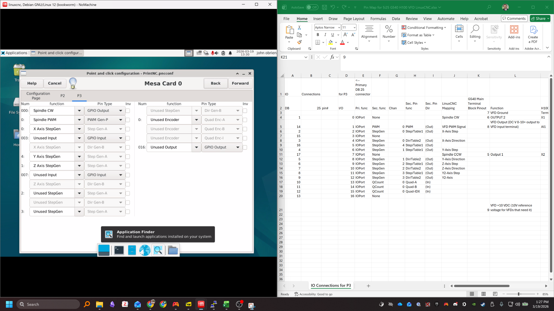
So far so good... Only when I look at the P3 tab in PnCConf, not all the I/O numbers from the output from the "sudo mesaflash --device 5i25 --readhmid" are listed (please see attached screenshot). Without all the I/O numbers listed, I don't understand how to properly set which functions should be selected for which pins.
Can I ask for some help please on how to properly use the PnCConf wizard in LinuxCNC to map my axis and spindle to the proper pins for the G540?
Regards,
John
I'm struggling to understand the configuration mapping window in the PnCConf Wizard.
I have flashed the 6i25 with the 5i25_g540x2.bit firmware and reloaded the firmware to make sure the new firmware is loaded.
Based of the manual for the 6i25 card, it looks like P3 is the tab to use to configure what each of the pins on the DB25 connector on the back of the machine does.
Based off this post , it looks like the "num" column in the P3 window is to be interpreted as a GPIO pin number if the number has two leading digits and a function or module number if the number has no leading digits.
I ran "sudo mesaflash --device 5i25 --readhmid" and got following output for P3:
IO Connections for P3
DB25 pin# I/O Pri. func Sec. func Chan Sec. Pin func Sec. Pin Dir
1 0 IOPort None
14 1 IOPort PWM 0 PWM (Out)
2 2 IOPort StepGen 0 Step/Table1 (Out)
15 3 IOPort None
3 4 IOPort StepGen 0 Dir/Table2 (Out)
16 5 IOPort StepGen 4 Step/Table1 (Out)
4 6 IOPort StepGen 1 Step/Table1 (Out)
17 7 IOPort None
5 8 IOPort StepGen 1 Dir/Table2 (Out)
6 9 IOPort StepGen 2 Step/Table1 (Out)
7 10 IOPort StepGen 2 Dir/Table2 (Out)
8 11 IOPort StepGen 3 Step/Table1 (Out)
9 12 IOPort StepGen 3 Dir/Table2 (Out)
10 13 IOPort QCount 0 Quad-A (In)
11 14 IOPort QCount 0 Quad-B (In)
12 15 IOPort QCount 0 Quad-IDX (In)
13 16 IOPort None
So far so good... Only when I look at the P3 tab in PnCConf, not all the I/O numbers from the output from the "sudo mesaflash --device 5i25 --readhmid" are listed (please see attached screenshot). Without all the I/O numbers listed, I don't understand how to properly set which functions should be selected for which pins.
Can I ask for some help please on how to properly use the PnCConf wizard in LinuxCNC to map my axis and spindle to the proper pins for the G540?
Regards,
John
Please Log in or Create an account to join the conversation.
- PCW
-

- Offline
- Moderator
-

Less
More
- Posts: 17971
- Thank you received: 5270
20 Mar 2026 02:02 - 20 Mar 2026 03:04 #344538
by PCW
Replied by PCW on topic Difficulty understanding configuration mapping window in PnCConf Wizard
Pncconf is a bit confusing because the num columm contains either channel
numbers (1 digit) or GPIO numbers (3 digits). One main thing to remember
is that you don't really need to care about the pin numbers for the main functions.
as the firmware maps these to the proper pins.
With G540 firmware the stepgens for example are mapped in a logical sequence:
0=G540 X
1=G540 Y
2=G540 Z
3=G540 A
So you just use the channel number "NUM" in pncconf to map the stepgens appropriately
Also you can get a list of G540 function to channel and GPIO pins with:
sudo measflash --device 5i25 --dbname1 g540 --readhmid
Last edit: 20 Mar 2026 03:04 by PCW.
Please Log in or Create an account to join the conversation.
- john.obrien
- Offline
- New Member
-
Less
More
- Posts: 13
- Thank you received: 4
20 Mar 2026 13:14 #344546
by john.obrien
Replied by john.obrien on topic Difficulty understanding configuration mapping window in PnCConf Wizard
Perfect. Thank you for your help!
Please Log in or Create an account to join the conversation.
- john.obrien
- Offline
- New Member
-
Less
More
- Posts: 13
- Thank you received: 4
22 Mar 2026 14:11 #344605
by john.obrien
Replied by john.obrien on topic Difficulty understanding configuration mapping window in PnCConf Wizard
If the Num column indicates channel if the numbers are one digit long, and the pins associated with the 0 channel are for the x-axis, why is the PWM signal for the spindle and associated encoders also on channel 0 in this
screenshot
of the PcCConf wizard?
Please Log in or Create an account to join the conversation.
- PCW
-
- Offline
- Moderator
-
Less
More
- Posts: 17971
- Thank you received: 5270
22 Mar 2026 15:35 - 22 Mar 2026 15:38 #344609
by PCW
Replied by PCW on topic Difficulty understanding configuration mapping window in PnCConf Wizard
All secondary pin function channels are numbered 0..N
(the primary function of each pin is GPIO)
So if you have 6 stepgens, they would be numbered 0 to 5.
And if you had 2 PWM generators or encoders they would be numbered 0 to 1.
(the primary function of each pin is GPIO)
So if you have 6 stepgens, they would be numbered 0 to 5.
And if you had 2 PWM generators or encoders they would be numbered 0 to 1.
Last edit: 22 Mar 2026 15:38 by PCW.
Please Log in or Create an account to join the conversation.
- john.obrien
- Offline
- New Member
-
Less
More
- Posts: 13
- Thank you received: 4
23 Mar 2026 15:26 #344640
by john.obrien
Replied by john.obrien on topic Difficulty understanding configuration mapping window in PnCConf Wizard
Ok, thanks PCW.
Please Log in or Create an account to join the conversation.
Moderators: cmorley
- Configuring LinuxCNC
- Configuration Tools
- PnCConf Wizard
- Difficulty understanding configuration mapping window in PnCConf Wizard
Time to create page: 0.127 seconds