Flash a XC6SLX9 dev board as a 7i90HD
- PCW
-

- Offline
- Moderator
-

Less
More
- Posts: 17961
- Thank you received: 5265
25 Apr 2019 20:29 #131883
by PCW
Replied by PCW on topic Flash a XC6SLX9 dev board as a 7i90HD
The proper card type (you should really use your own name here) and pinout file must be included in the top level file
In addition, any source file used must be added to the project
(right click in file window and add if they are not listed)
In addition, any source file used must be added to the project
(right click in file window and add if they are not listed)
Please Log in or Create an account to join the conversation.
- dm17ry
-

- Offline
- Elite Member
-

Less
More
- Posts: 207
- Thank you received: 89
25 Apr 2019 22:50 #131897
by dm17ry
Replied by dm17ry on topic Flash a XC6SLX9 dev board as a 7i90HD
PCW, a bit off topic.
but i was wondering... there's no PCI setup/hold timing constraints in the 5i25.ucf or elsewhere. how do you get away without them?
but i was wondering... there's no PCI setup/hold timing constraints in the 5i25.ucf or elsewhere. how do you get away without them?
Please Log in or Create an account to join the conversation.
- PCW
-
- Offline
- Moderator
-
Less
More
- Posts: 17961
- Thank you received: 5265
25 Apr 2019 23:50 - 25 Apr 2019 23:54 #131904
by PCW
Replied by PCW on topic Flash a XC6SLX9 dev board as a 7i90HD
They should be there, my oversight, though its not really possible to violate the
PCI specs rather generous 7 ns setup, 0 ns hold and 11 ns output offset specs at 33 MHz with one wait state.
Also the Async TRDY, DEVSEL and STOP signals should have pad-pad times
(more likely to be an issue at 66MHz)
I will look into adding these
PCI specs rather generous 7 ns setup, 0 ns hold and 11 ns output offset specs at 33 MHz with one wait state.
Also the Async TRDY, DEVSEL and STOP signals should have pad-pad times
(more likely to be an issue at 66MHz)
I will look into adding these
Last edit: 25 Apr 2019 23:54 by PCW.
Please Log in or Create an account to join the conversation.
- dm17ry
-
- Offline
- Elite Member
-
Less
More
- Posts: 207
- Thank you received: 89
26 Apr 2019 00:36 - 26 Apr 2019 00:41 #131910
by dm17ry
Replied by dm17ry on topic Flash a XC6SLX9 dev board as a 7i90HD
thank you for clarification! have to study your PCI implementation... my PCI core implementation attempt effortlessly miss that generous 11ns output offset budget by 3ns on AD pins. among other less severe violations ")
Last edit: 26 Apr 2019 00:41 by dm17ry.
Please Log in or Create an account to join the conversation.
- gtt38
- Offline
- Senior Member
-

Less
More
- Posts: 79
- Thank you received: 4
02 May 2019 09:09 - 02 May 2019 09:34 #132498
by gtt38
Replied by gtt38 on topic Flash a XC6SLX9 dev board as a 7i90HD
I want to thank you again PCW.
I read 2 books on VHDL and i understood a little bit more the code, and it's beatifully written.
Now i can compile every firmware i want, i'm better with ISE.
I discovered many things during these fews days, i really thing that my boad has a counterfeit XC6SLX9. You can find it for 3$ in China maybe less if ordered in quantity. That's why you could have this dev board for less than 20$. So my advice is to avoid this kind of products.
So i decided to create my own design with a genuine XC6SLX9-2TQG144C, totally open source to make my experimentations with MCU. It's a really simple board with simple specifications : 100x100mm 2 layers, 72 I/O on 3 connectors (mesa daughter compatible) with 3x FST16211, a SPI interface and a 16Mbit flash.
Since i'm not familiar with FPGA i'll need your help to correct my mistakes.
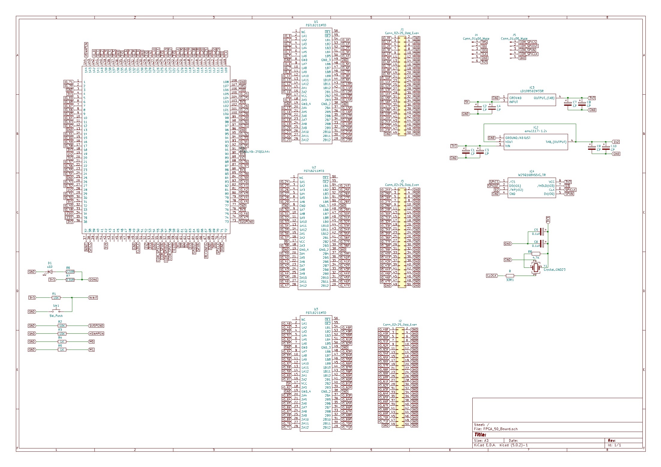
After reading the FST16211 datasheet i think I inverted I/O, how can i drive enable pins too ?
Do i have to protect the SPI too ? Maybe with a 8bits TTL like the FST16211 ?
And many other questions like what's the use of these pins :
_ pin 37
_ pin 59
_ pin 60
_ pin 69
_ pin 67
_ pin 73
_ pin 144
I read 2 books on VHDL and i understood a little bit more the code, and it's beatifully written.
Now i can compile every firmware i want, i'm better with ISE.
I discovered many things during these fews days, i really thing that my boad has a counterfeit XC6SLX9. You can find it for 3$ in China maybe less if ordered in quantity. That's why you could have this dev board for less than 20$. So my advice is to avoid this kind of products.
So i decided to create my own design with a genuine XC6SLX9-2TQG144C, totally open source to make my experimentations with MCU. It's a really simple board with simple specifications : 100x100mm 2 layers, 72 I/O on 3 connectors (mesa daughter compatible) with 3x FST16211, a SPI interface and a 16Mbit flash.
Since i'm not familiar with FPGA i'll need your help to correct my mistakes.
After reading the FST16211 datasheet i think I inverted I/O, how can i drive enable pins too ?
Do i have to protect the SPI too ? Maybe with a 8bits TTL like the FST16211 ?
And many other questions like what's the use of these pins :
_ pin 37
_ pin 59
_ pin 60
_ pin 69
_ pin 67
_ pin 73
_ pin 144
Attachments:
Last edit: 02 May 2019 09:34 by gtt38.
Please Log in or Create an account to join the conversation.
- InMyDarkestHour
-

- Visitor
-

02 May 2019 09:26 #132500
by InMyDarkestHour
Replied by InMyDarkestHour on topic Flash a XC6SLX9 dev board as a 7i90HD
I don't know if this is any use, but I found this
numato.com/product/mimas-spartan-6-fpga-development-board
And the design files here
github.com/numato/samplecode/tree/master/FPGA/Mimas
numato.com/product/mimas-spartan-6-fpga-development-board
And the design files here
github.com/numato/samplecode/tree/master/FPGA/Mimas
Please Log in or Create an account to join the conversation.
- gtt38
- Offline
- Senior Member
-
Less
More
- Posts: 79
- Thank you received: 4
02 May 2019 09:38 #132501
by gtt38
Replied by gtt38 on topic Flash a XC6SLX9 dev board as a 7i90HD
Thank you
I already checked these schematics like many other XC6SLX9 dev boards but it's not helping for this specific use.
I already checked these schematics like many other XC6SLX9 dev boards but it's not helping for this specific use.
Please Log in or Create an account to join the conversation.
- InMyDarkestHour
-
- Visitor
-
02 May 2019 10:50 #132509
by InMyDarkestHour
Replied by InMyDarkestHour on topic Flash a XC6SLX9 dev board as a 7i90HD
Regarding Pins
Is this of any help ?
www.xilinx.com/support/documentation/use...es/ug385.pdf#page=19
Is this of any help ?
www.xilinx.com/support/documentation/use...es/ug385.pdf#page=19
Please Log in or Create an account to join the conversation.
- gtt38
- Offline
- Senior Member
-
Less
More
- Posts: 79
- Thank you received: 4
02 May 2019 13:32 - 02 May 2019 13:33 #132535
by gtt38
Replied by gtt38 on topic Flash a XC6SLX9 dev board as a 7i90HD
A little bit thank you. I will follow the same specifications as my dev board for these pins.
I will need advices for the 50mhz crystal too
I will need advices for the 50mhz crystal too
Last edit: 02 May 2019 13:33 by gtt38.
Please Log in or Create an account to join the conversation.
- InMyDarkestHour
-
- Visitor
-
03 May 2019 01:57 #132590
by InMyDarkestHour
Replied by InMyDarkestHour on topic Flash a XC6SLX9 dev board as a 7i90HD
I think you will have to read the Xilinx docs.....especially UG393 regarding PCB design, there's quite a few docs to go through.
Not as straight forward as designing for a simple adruino type project. Keep going you have an interesting project going on.
Not as straight forward as designing for a simple adruino type project. Keep going you have an interesting project going on.
Please Log in or Create an account to join the conversation.
Moderators: PCW, jmelson
Time to create page: 0.519 seconds