Flash a XC6SLX9 dev board as a 7i90HD
- Boaschti
- Offline
- Junior Member
-

- Posts: 23
- Thank you received: 2
I hope somebody can help me.
I have a rpi3 connected with GPIO 24, 25, 26 & 27 to TDO, TCK, TDI, TMS and SPI GPIO 8, 9, 10, 11 to P14, P15, P16, P132
The 50MHz oszillator is on P50.
I want to programm the 7c80d.bit file. Programming the File with openocd looks good.
Mesaflash output says:root@raspberrypi:/home/pi# openocd -f /usr/local/share/openocd/scripts/interface/raspberrypi2-native.cfg -f /usr/local/share/openocd/scripts/cpld/xilinx-xc6s.cfg -c "init; xc6s_program xc6s.tap; pld load 0 /home/pi/7c80d.bit; exit"
Open On-Chip Debugger 0.11.0+dev-00550-gd27d66bc1 (2022-01-04-20:33)
Licensed under GNU GPL v2
For bug reports, read
openocd.org/doc/doxygen/bugs.html
DEPRECATED! use 'adapter speed' not 'adapter_khz'
adapter speed: 250 kHz
Info : auto-selecting first available session transport "jtag". To override use 'transport select <transport>'.
xc6s_print_dna
Info : BCM2835 GPIO JTAG/SWD bitbang driver
Info : clock speed 250 kHz
Info : JTAG tap: xc6s.tap tap/device found: 0x24001093 (mfg: 0x049 (Xilinx), part: 0x4001, ver: 0x2)
Warn : gdb services need one or more targets defined
root@raspberrypi:/home/pi#
I have an SPI output from RPI3 but from FPGA in my opinion nothing useable.root@raspberrypi:/home/pi# mesaflash --spi --device 7c80 --addr /dev/spidev0.0 --fix-boot-block --verbose unable to set bpw32, fallback to bpw8
Unexpected cookie at 0100..0110:
00000000 00000000 00000000
No 7C80 board found
I set the SPI speed form mesaflash to 200khz to prevent timing prevent capacitive errors.
What is a that cookie?
Any idea why it does not work?
Best regards.
Attachments:
Please Log in or Create an account to join the conversation.
- PCW
-

- Offline
- Moderator
-

- Posts: 17864
- Thank you received: 5231
2. Lowering the clock speed will not help (its the clock signal fidelity that matters as long as it's not higher than 24 MHz or so)
Please Log in or Create an account to join the conversation.
- Boaschti
- Offline
- Junior Member
-

- Posts: 23
- Thank you received: 2
Please Log in or Create an account to join the conversation.
- PCW
-

- Offline
- Moderator
-

- Posts: 17864
- Thank you received: 5231
Please Log in or Create an account to join the conversation.
- Boaschti
- Offline
- Junior Member
-

- Posts: 23
- Thank you received: 2
Please Log in or Create an account to join the conversation.
- ALittleOffTheRails
-

- Visitor
-

Would this have any impact on the function of this board.
Schematics below if anyone would like to look.
Please Log in or Create an account to join the conversation.
- Gene1934
- Offline
- Elite Member
-

- Posts: 174
- Thank you received: 13
Is that planned to be a separate probably passive board? The 50 pin idc sockets on the real 7i90HD are a pita, only really usable as take off points to connect the 7i42TA's with 2 or 4" long cables. Since I do not currantly have a fully functional 7i90HD, one of the stepgens is blown, I would be interested in such a setup that would also function with a bananapi-m5, which can run at 2GHz, has no radio, but all 4 usb portrs are usb3. Currently using a pile of them to drive 3d printers. I have visions of a tool changer that would need the 4th stepgen. I'm currently running on an rpi4b, a 7i90HD, and 3 7i42TA's with a Spin-X1 driving a vfd for spindle control.
Please keep me advised.
Cheers, Gene Heskett
--
"There are four boxes to be used in defense of liberty:
soap, ballot, jury, and ammo. Please use in that order."
-Ed Howdershelt (Author)
Genes Web page <geneslinuxbox.net:6309/gene>
Please Log in or Create an account to join the conversation.
- Cant do this anymore bye all
-

- Offline
- Platinum Member
-

- Posts: 1200
- Thank you received: 425
Have you tried one of the banana 5 boards with a 7i90 using the hm2_spi driver. I tried with the latest Raspberry Pi 5 and it keep erroring with SPI timeouts. The hm2_rpspi driver doesn't work at all.
I hooked back up to my RP-400 and the hm2_spi driver ok. The hm2_rpspi does work on it fine.
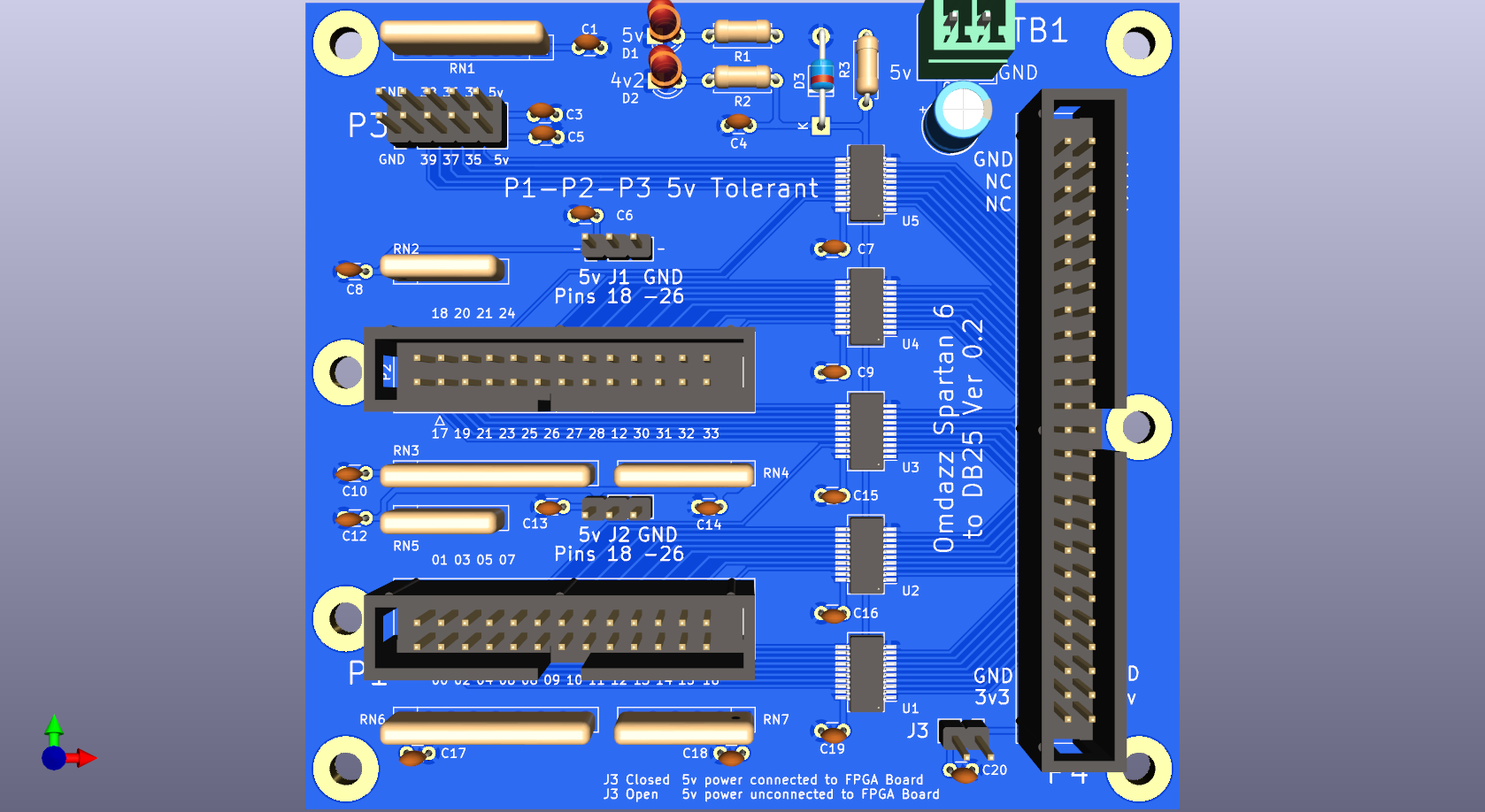
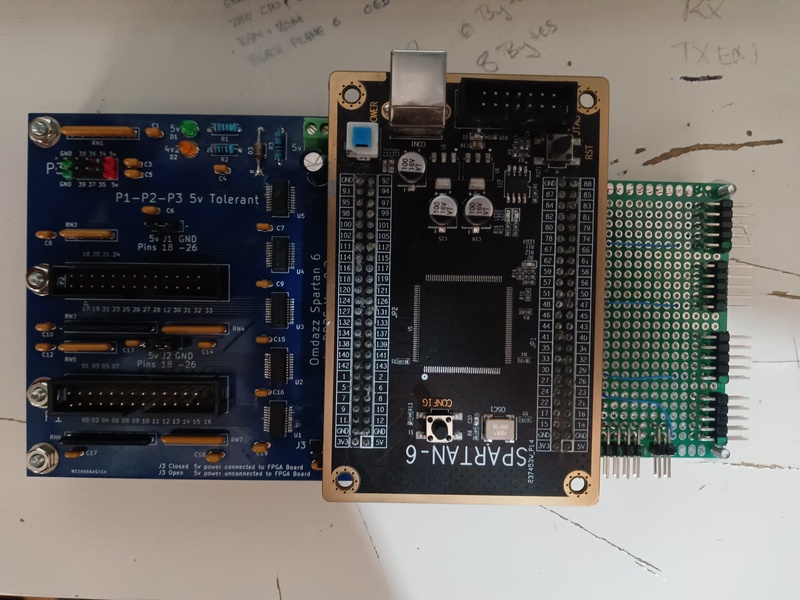
I've got a couple of prototype boards that work with the same Dev board which is about AUD $70 dollars now. It has the FET bus switches and has 2xDB25 connectors that will work with a standard Parallel Port breakout board or with the Mesa DB25 boards. There's also a 2*5 pin header that gives you 6 extra GPIOs with GND & 5v. That's the board that connects to the left hand header if you look at the dev board with the USB connector at the top.
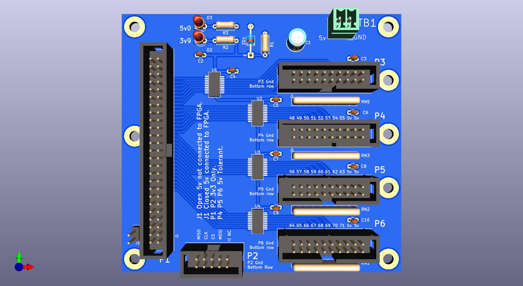
The second board has the SPI connector 2x5 so that there's a ground wire between each signal. Then there's 4 of 2x10 connectors that have 8 GPIOs 5v power on the top 10 pins and ground on the bottom 10 pins.
On all boards the signal from the FPGA are routed through a get bus switch running on a 3.9v power rail, and on the "world side" pulled up to 5v, this gives about 3.2~ volts on the FPGA side . Pretty much the way Mesa do things.
The only smd parts are the bus switches everything else is through hole, makes assembly easier. Too many dollars to get the PCB fab house to assemble the board.
Please Log in or Create an account to join the conversation.
- Gene1934
- Offline
- Elite Member
-

- Posts: 174
- Thank you received: 13
That I suspect is because the address of the gpio controller doesn't match the rpi4b address. With a genuine rpi4b the rpspi driver works flawlessly. Bertho Stultans, a cs prof at a swedish uni was kind enough to write that driver, and rewrite for the rpi4b when it came out. Perhaps he would supply an include file to make it work with the bpi5, IDK and have not had any correspondence with him since, no need to as it just works, sending 32 bit packet at 42 megabaud and receiving the replies from the 7i90HD at 25 megabaud. My spi cable is maybe 1.25" long as I turned the pi upside down so the connecters were pin aligned. And old 12 volt fan, borrowed from a defunct video card running on 5 volts and mounted under the pi is all the cooling its needed in around 5 years. And my copy of the docs says its directly connected to the fpga, no buffers.
If Peter has since modified it to provide 5 v tolerant buffers, he hasn't told me.
Cheers, Gene Heskett
--
"There are four boxes to be used in defense of liberty:
soap, ballot, jury, and ammo. Please use in that order."
-Ed Howdershelt (Author)
Genes Web page <geneslinuxbox.net:6309/gene>
Please Log in or Create an account to join the conversation.
- Cant do this anymore bye all
-

- Offline
- Platinum Member
-

- Posts: 1200
- Thank you received: 425
Some rendering of the boards I described, the dev board had the header pins changed to female and located on the underside.
Board 1:
Board 2:
Dev board with board 1 & prototype board 2
Attachments:
Please Log in or Create an account to join the conversation.


