I want to thank you again PCW.
I read 2 books on VHDL and i understood a little bit more the code, and it's beatifully written.
Now i can compile every firmware i want, i'm better with ISE.
I discovered many things during these fews days, i really thing that my boad has a counterfeit XC6SLX9. You can find it for 3$ in China maybe less if ordered in quantity. That's why you could have this dev board for less than 20$. So my advice is to avoid this kind of products.
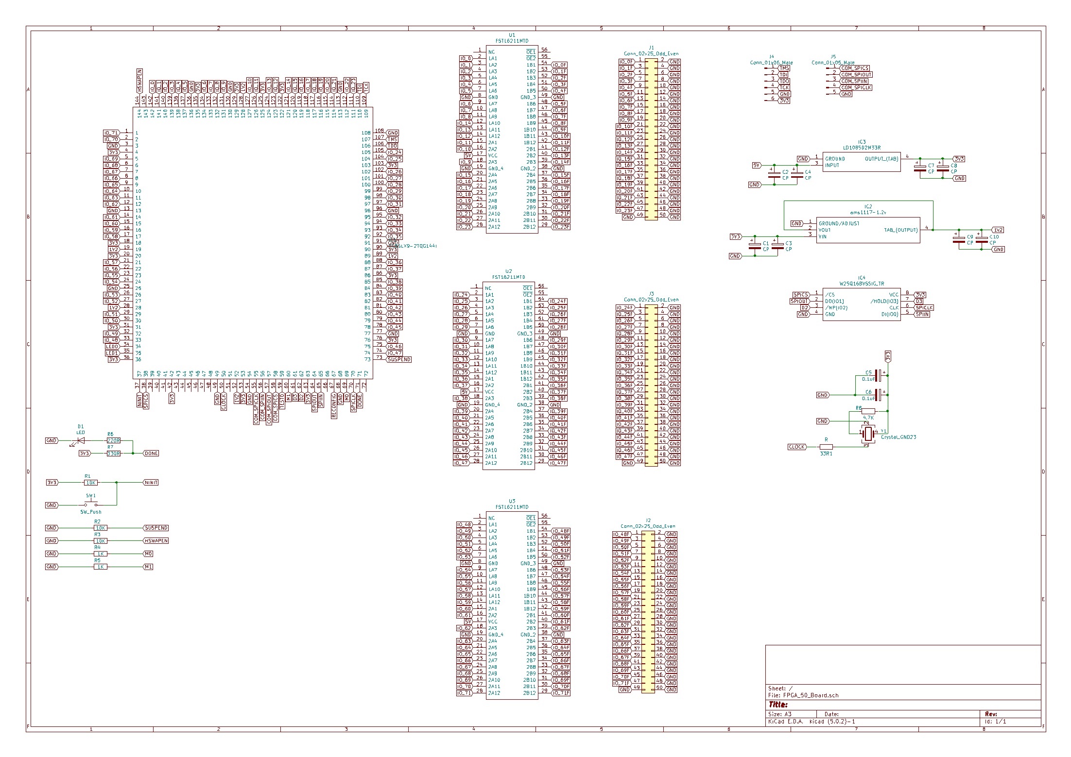
So i decided to create my own design with a genuine XC6SLX9-2TQG144C, totally open source to make my experimentations with MCU. It's a really simple board with simple specifications : 100x100mm 2 layers, 72 I/O on 3 connectors (mesa daughter compatible) with 3x FST16211, a SPI interface and a 16Mbit flash.
Since i'm not familiar with FPGA i'll need your help to correct my mistakes.
After reading the FST16211 datasheet i think I inverted I/O, how can i drive enable pins too ?
Do i have to protect the SPI too ? Maybe with a 8bits TTL like the FST16211 ?
And many other questions like what's the use of these pins :
_ pin 37
_ pin 59
_ pin 60
_ pin 69
_ pin 67
_ pin 73
_ pin 144