5i25/6i25 bitfile for DMB4350-8B bob
- PCW
-

- Offline
- Moderator
-

Less
More
- Posts: 17917
- Thank you received: 5246
12 Feb 2021 00:52 - 12 Feb 2021 00:54 #198466
by PCW
Replied by PCW on topic 5i25/6i25 bitfile for DMB4350-8B bob
On the configuration page, make sure you select only the number of stepgens,
pwmgens, and encoders you will use (to free the pins for GPIO use)
pncconf lists both the GPIO numbers (3 digits) and module numbers ( 1 digit like stepgen 0,1,2,3 etc)
in the first column so its a bit confusing. Normally standard firmware will assign stepgens in a sensible
fashion so 0=X on BOB, 1 = Y, 2 = Z etc
Last edit: 12 Feb 2021 00:54 by PCW.
Please Log in or Create an account to join the conversation.
- PCW
-
- Offline
- Moderator
-
Less
More
- Posts: 17917
- Thank you received: 5246
12 Feb 2021 01:05 #198467
by PCW
Replied by PCW on topic 5i25/6i25 bitfile for DMB4350-8B bob
Normally you would assign stepgens something like this:
For the I/O on P3 you would need to look at the pinout file
to get the DB25 <-> GPIO conversions to know which
GPIO matches which BOB pin
For the I/O on P3 you would need to look at the pinout file
to get the DB25 <-> GPIO conversions to know which
GPIO matches which BOB pin
Please Log in or Create an account to join the conversation.
- 0jw
- Offline
- Premium Member
-

Less
More
- Posts: 98
- Thank you received: 0
12 Feb 2021 01:18 #198470
by 0jw
Replied by 0jw on topic 5i25/6i25 bitfile for DMB4350-8B bob
i dont think this is going to work for the dmm pinout. its missing pin 2 and pin 3
Please Log in or Create an account to join the conversation.
- PCW
-
- Offline
- Moderator
-
Less
More
- Posts: 17917
- Thank you received: 5246
12 Feb 2021 01:24 #198471
by PCW
Replied by PCW on topic 5i25/6i25 bitfile for DMB4350-8B bob
DB25 pins 2 and 3 are assigned to stepgen 0:
IO Connections for P3
Pin#  I/O   Pri. func    Sec. func       Chan      Pin func        Pin Dir

 1      0   IOPort       PWMGen           0        PWM             (Out)
14      1   IOPort       None
 2      2   IOPort       StepGen          0        Dir             (Out) <<<<<<<<<<<<<<<<<
15      3   IOPort       None
 3      4   IOPort       StepGen          0        Step            (Out) <<<<<<<<<<<<<<<<<
16      5   IOPort       None
 4      6   IOPort       StepGen          1        Dir             (Out)
17      7   IOPort       None
 5      8   IOPort       StepGen          1        Step            (Out)
 6      9   IOPort       StepGen          2        Dir             (Out)
 7     10   IOPort       StepGen          2        Step            (Out)
 8     11   IOPort       StepGen          3        Dir             (Out)
 9     12   IOPort       StepGen          3        Step            (Out)
10     13   IOPort       None
11     14   IOPort       QCount           0        Quad-A          (In)
12     15   IOPort       QCount           0        Quad-B          (In)
13     16   IOPort       QCount           0        Quad-IDX        (In)
Please Log in or Create an account to join the conversation.
- 0jw
- Offline
- Premium Member
-
Less
More
- Posts: 98
- Thank you received: 0
12 Feb 2021 01:53 #198472
by 0jw
Replied by 0jw on topic 5i25/6i25 bitfile for DMB4350-8B bob
thank you. I don't understand what the purpose of IO connector 2 and IO connector 3 is? some "Num:" are in both. maybe I should remove the keyed molex connectors on the board and replace it with screw terminals. otherwise im stuck with that pin configuration. or make a new db25 cable
Please Log in or Create an account to join the conversation.
- PCW
-
- Offline
- Moderator
-
Less
More
- Posts: 17917
- Thank you received: 5246
12 Feb 2021 02:47 - 12 Feb 2021 02:47 #198473
by PCW
Replied by PCW on topic 5i25/6i25 bitfile for DMB4350-8B bob
IO connector 3 is P3 on a 5I25 or 6I25 (the DB25 on the bracket end of the card),
which in all you need to configure unless you are using 2 BOBs
The pinout should be correct, why would you change any wiring?
which in all you need to configure unless you are using 2 BOBs
The pinout should be correct, why would you change any wiring?
Last edit: 12 Feb 2021 02:47 by PCW.
Please Log in or Create an account to join the conversation.
- 0jw
- Offline
- Premium Member
-
Less
More
- Posts: 98
- Thank you received: 0
12 Feb 2021 03:09 - 12 Feb 2021 03:10 #198474
by 0jw
Replied by 0jw on topic 5i25/6i25 bitfile for DMB4350-8B bob
on I/O conector i only have
000:
0:
0:
003:
1:
007:
2:
3:
013:
0:
000:
0:
0:
003:
1:
007:
2:
3:
013:
0:
Last edit: 12 Feb 2021 03:10 by 0jw.
Please Log in or Create an account to join the conversation.
- PCW
-
- Offline
- Moderator
-
Less
More
- Posts: 17917
- Thank you received: 5246
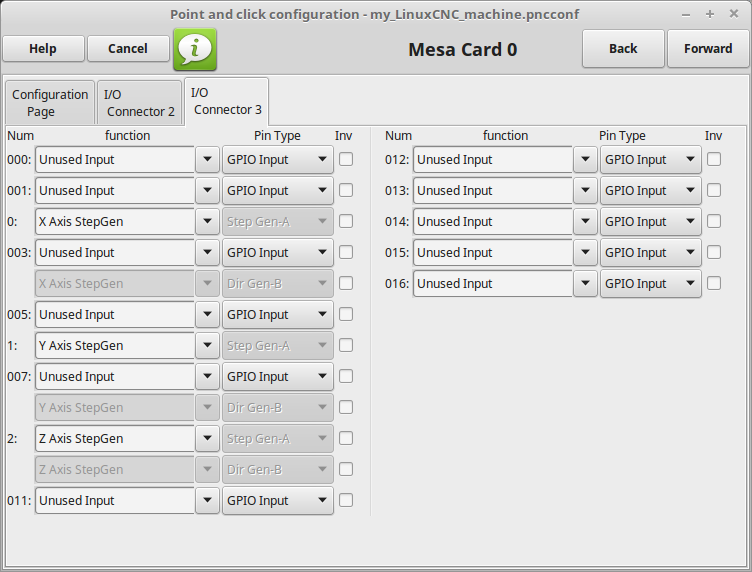
12 Feb 2021 03:22 #198475
by PCW
Replied by PCW on topic 5i25/6i25 bitfile for DMB4350-8B bob
it should look like my image
if you
1. Select 5i25 with internal firmware prob_rfx2
2. Set the number of encoders and PWM gens to 0
3. Select accept component changes
4 look at the IO connector 3 tab
if you
1. Select 5i25 with internal firmware prob_rfx2
2. Set the number of encoders and PWM gens to 0
3. Select accept component changes
4 look at the IO connector 3 tab
Please Log in or Create an account to join the conversation.
- 0jw
- Offline
- Premium Member
-
Less
More
- Posts: 98
- Thank you received: 0
12 Feb 2021 03:31 #198476
by 0jw
Replied by 0jw on topic 5i25/6i25 bitfile for DMB4350-8B bob
ok that looks to be the same. not sure how it will work with my pin out
Please Log in or Create an account to join the conversation.
- 0jw
- Offline
- Premium Member
-
Less
More
- Posts: 98
- Thank you received: 0
12 Feb 2021 03:34 #198477
by 0jw
Replied by 0jw on topic 5i25/6i25 bitfile for DMB4350-8B bob
i tried the test run and nothing happen
Please Log in or Create an account to join the conversation.
Time to create page: 0.161 seconds