
Search Results (Searched for: )
- tuxcnc
- tuxcnc
04 Oct 2026 08:45
Replied by tuxcnc on topic Standalone LinuxCNC machine simulator using the Stepper-Ninja HAL interface
Standalone LinuxCNC machine simulator using the Stepper-Ninja HAL interface
Category: General LinuxCNC Questions
First, a gift - a script that launches both windows with one click.Everything seems to be working, but I found some errors in the settings.
Usually the Z axis looks for the limit switch at the top, here it goes down... You need to change the sign of the HOME_SEARCH_VELOCITY value to the opposite.
The work area is set to extremely small, it is unlikely that the real work will fit. When changing the field, you also need to set virtual limits.
And the worst thing is that I have an offset of several millimeters in the Z axis between Axis and the simulator. I don't know where this comes from. Of course, you can add some value in the material settings, but this is not very elegant.
#!/bin/bash
# change path in next line if needs
cd /usr/src/linuxcnc-sim
./scripts/setup-veth.sh
bash -c 'xfce4-terminal -x ip netns exec cnc-sim-ns   runuser -u "$USER" -- env   DISPLAY="$DISPLAY"   XAUTHORITY="${XAUTHORITY:-$HOME/.Xauthority}"   XDG_RUNTIME_DIR="${XDG_RUNTIME_DIR:-/run/user/$(id -u)}"   ./build/cnc-sim --config examples/mill/simulator.ini'
linuxcnc examples/phase3/phase3.iniUsually the Z axis looks for the limit switch at the top, here it goes down... You need to change the sign of the HOME_SEARCH_VELOCITY value to the opposite.
The work area is set to extremely small, it is unlikely that the real work will fit. When changing the field, you also need to set virtual limits.
And the worst thing is that I have an offset of several millimeters in the Z axis between Axis and the simulator. I don't know where this comes from. Of course, you can add some value in the material settings, but this is not very elegant.
- tuxcnc
- tuxcnc
04 Oct 2026 06:34
Replied by tuxcnc on topic Mesa Ethernet / QtPlasmaC retrofit experience — lessons from a marginal mini PC
Mesa Ethernet / QtPlasmaC retrofit experience — lessons from a marginal mini PC
Category: Computers and Hardware
Choosing a computer for LinuxCNC is always a lottery and it is impossible to give any universal advice.
A computer that works great for you may not work for me with my version of Linux, my version of kernel and my version of LinuxCNC...
For example, I use AMD computers (A10 and Ryzen), also with Realtec NIC and MESA. I have read several times on this forum that they do not and will not work with LinuxCNC and especially MESA, but they work flawlessly and I am very happy with them.
Even if you gave a specific computer model, motherboard revision, operating system type, kernel version, LinuxCNC version, it would make some sense, but tomorrow some developer will change something and something may stop working...
A computer that works great for you may not work for me with my version of Linux, my version of kernel and my version of LinuxCNC...
For example, I use AMD computers (A10 and Ryzen), also with Realtec NIC and MESA. I have read several times on this forum that they do not and will not work with LinuxCNC and especially MESA, but they work flawlessly and I am very happy with them.
Even if you gave a specific computer model, motherboard revision, operating system type, kernel version, LinuxCNC version, it would make some sense, but tomorrow some developer will change something and something may stop working...
- tommylight
04 Oct 2026 02:49
Replied by tommylight on topic Mesa Ethernet / QtPlasmaC retrofit experience — lessons from a marginal mini PC
Mesa Ethernet / QtPlasmaC retrofit experience — lessons from a marginal mini PC
Category: Computers and Hardware
You are welcomed, always.
P.S.
Wait till you figure out what you can do in HAL !
That is the main thing why i liked it so much back then, for me it just clicks "connect this pin to this pin" and it works!
P.S.
Wait till you figure out what you can do in HAL !
That is the main thing why i liked it so much back then, for me it just clicks "connect this pin to this pin" and it works!
- trackwhack
- trackwhack
04 Oct 2026 02:17
Replied by trackwhack on topic Perpetual License CAM
Perpetual License CAM
Category: Show Your Stuff
Hi @dbtayl,
Except for the adaptive clearing issue you are facing (unable to clear outside model) , we were able to replicate everything else and make the necessary changes.
You can save it as a project file and mail it to This email address is being protected from spambots. You need JavaScript enabled to view it.
Thank you for your help.
Kind Regards,
George
Except for the adaptive clearing issue you are facing (unable to clear outside model) , we were able to replicate everything else and make the necessary changes.
You can save it as a project file and mail it to This email address is being protected from spambots. You need JavaScript enabled to view it.
Thank you for your help.
Kind Regards,
George
- FabLabRacing
- FabLabRacing
04 Oct 2026 01:35 - 04 Oct 2026 01:36
Replied by FabLabRacing on topic Mesa Ethernet / QtPlasmaC retrofit experience — lessons from a marginal mini PC
Mesa Ethernet / QtPlasmaC retrofit experience — lessons from a marginal mini PC
Category: Computers and Hardware
**A Few Months With LinuxCNC / QtPlasmaC — Follow-Up and Thank You**
Back in July, I posted about the PC and realtime issues I encountered while converting my home-built plasma table from MASSO to LinuxCNC / QtPlasmaC. Now that I have been using it for a few months, I wanted to follow up and, more importantly, thank the LinuxCNC community.
The short version is that I am very happy I made the conversion.
At this point I have cut roughly a dozen actual parts and spent a large number of hours setting up the machine, troubleshooting it, experimenting with it, and generally just playing with it. None of those hours were wasted.
The Dell OptiPlex 7060 with Intel Ethernet has proven to be the “boring” control PC I was looking for. After some additional tuning, including CPU isolation and changes to how my camera project delivers frames, I have been able to run QtPlasmaC and FabScan together for hours without realtime, Mesa, watchdog, or Smart Serial faults.
I still stand behind the main point of my original post: with Mesa Ethernet, the details of the PC matter more than raw horsepower. The NIC, driver, BIOS and power-management behavior, and long-term realtime stability are more important than whether the computer looks powerful on paper. A modest business-class PC with Intel Ethernet has worked much better for me than the newer mini PC I originally tried.
What has changed since July is my understanding of LinuxCNC itself.
LinuxCNC / QtPlasmaC can definitely be challenging to set up and dial in. There are a lot of layers, and there are plenty of opportunities to configure something incorrectly. At first, that can make it seem unpredictable.
After working with it for a while, I have found the opposite to be true. LinuxCNC is actually very predictable. When something does not work, there is normally a logical reason for it. It may be a signal polarity, a HAL connection, a configuration path, a file permission, a post-processor issue, or a setting I did not completely understand, but there is usually an identifiable cause.
More importantly, LinuxCNC gives me the tools to find that cause. I can look at the HAL signals, see the machine state, follow what the controller is doing, and change the logic when necessary. Once I began to understand how the pieces fit together, troubleshooting became much less intimidating.
I also think LinuxCNC is easier to get into now than it was a few years ago. One of my previous problems with Linux-based projects was that a traditional Google search would often return information that was several versions out of date. AI-assisted searches have helped me sort through that, especially when I include the specific LinuxCNC and QtPlasmaC versions in the question.
The documentation also seems better than I remember, although it is possible I am just getting older, slowing down, and actually reading it this time.
The QtPlasmaC feature set has lived up to my original expectations. The material handling, probing, THC operation and visibility, Arc OK handling, cut recovery, scribing, hole processing, and operator feedback all feel like they were designed specifically for plasma cutting rather than added to a general-purpose CNC interface afterward.
Cut recovery is probably one of my favorite examples. If a cut stops, I can use Reverse to back up along the actual cut path, stop wherever I want, and press Cycle Start. QtPlasmaC then performs the normal plasma-start sequence, including waiting for Arc OK before continuing. When cutting larger parts, that is a very useful production feature rather than just a convenience.
The openness has also allowed me to do things that would be difficult or impossible with a closed controller. I was able to connect and configure my existing MASSO MPG pendant through the Mesa card, integrate the THCAD-2, customize the QtPlasmaC interface, and continue developing FabScan alongside the machine control.
FabScan was one of the main reasons I started looking at LinuxCNC in the first place. It uses a USB camera mounted to the machine and LinuxCNC motion to trace existing parts and templates, with the eventual goal of exporting usable geometry. It is still very much an ongoing experiment, but LinuxCNC gives me access to the machine state and motion control needed to build it. I am not limited to whatever features the controller manufacturer decided to include.
For perspective, I have used GRBL, ChiliPeppr/TinyG, Mach3, Mach4, MASSO, Langmuir Systems’ MR-1 Cut Control, and now LinuxCNC. If I build another CNC machine, I am almost positive it will be a LinuxCNC machine.
That is not because I now think every other controller is bad. MASSO, for example, remains a very solid and reliable controller. For someone who wants an appliance-like system, does not need much customization, and stays within the intended configuration, it is extremely easy to recommend.
The difference, in my opinion, can be summed up this way:
MASSO is easier until you need something it does not support.
LinuxCNC is harder until you understand it—then very little is off-limits.
Finally, I want to thank the LinuxCNC community.
A project like this only exists because people contribute their time to writing the software, developing QtPlasmaC, maintaining the documentation, designing hardware such as the Mesa cards, and answering questions from people like me who are still learning how all the pieces fit together.
The help I received made a real difference. Even when the answer turned out to be a single setting, an inverted input, or changing a 1 to a 0 after several hours of troubleshooting, someone was willing to help explain what that setting actually did and why it mattered.
When I wrote the original post in July, I hoped my experience might help the next person avoid a few days of chasing intermittent PC and realtime gremlins. After a few months of real use, my conclusion is that the “boring PC” advice still stands—but LinuxCNC / QtPlasmaC has absolutely been worth the effort.
Thank you to everyone who helped me get this far.
Back in July, I posted about the PC and realtime issues I encountered while converting my home-built plasma table from MASSO to LinuxCNC / QtPlasmaC. Now that I have been using it for a few months, I wanted to follow up and, more importantly, thank the LinuxCNC community.
The short version is that I am very happy I made the conversion.
At this point I have cut roughly a dozen actual parts and spent a large number of hours setting up the machine, troubleshooting it, experimenting with it, and generally just playing with it. None of those hours were wasted.
The Dell OptiPlex 7060 with Intel Ethernet has proven to be the “boring” control PC I was looking for. After some additional tuning, including CPU isolation and changes to how my camera project delivers frames, I have been able to run QtPlasmaC and FabScan together for hours without realtime, Mesa, watchdog, or Smart Serial faults.
I still stand behind the main point of my original post: with Mesa Ethernet, the details of the PC matter more than raw horsepower. The NIC, driver, BIOS and power-management behavior, and long-term realtime stability are more important than whether the computer looks powerful on paper. A modest business-class PC with Intel Ethernet has worked much better for me than the newer mini PC I originally tried.
What has changed since July is my understanding of LinuxCNC itself.
LinuxCNC / QtPlasmaC can definitely be challenging to set up and dial in. There are a lot of layers, and there are plenty of opportunities to configure something incorrectly. At first, that can make it seem unpredictable.
After working with it for a while, I have found the opposite to be true. LinuxCNC is actually very predictable. When something does not work, there is normally a logical reason for it. It may be a signal polarity, a HAL connection, a configuration path, a file permission, a post-processor issue, or a setting I did not completely understand, but there is usually an identifiable cause.
More importantly, LinuxCNC gives me the tools to find that cause. I can look at the HAL signals, see the machine state, follow what the controller is doing, and change the logic when necessary. Once I began to understand how the pieces fit together, troubleshooting became much less intimidating.
I also think LinuxCNC is easier to get into now than it was a few years ago. One of my previous problems with Linux-based projects was that a traditional Google search would often return information that was several versions out of date. AI-assisted searches have helped me sort through that, especially when I include the specific LinuxCNC and QtPlasmaC versions in the question.
The documentation also seems better than I remember, although it is possible I am just getting older, slowing down, and actually reading it this time.
The QtPlasmaC feature set has lived up to my original expectations. The material handling, probing, THC operation and visibility, Arc OK handling, cut recovery, scribing, hole processing, and operator feedback all feel like they were designed specifically for plasma cutting rather than added to a general-purpose CNC interface afterward.
Cut recovery is probably one of my favorite examples. If a cut stops, I can use Reverse to back up along the actual cut path, stop wherever I want, and press Cycle Start. QtPlasmaC then performs the normal plasma-start sequence, including waiting for Arc OK before continuing. When cutting larger parts, that is a very useful production feature rather than just a convenience.
The openness has also allowed me to do things that would be difficult or impossible with a closed controller. I was able to connect and configure my existing MASSO MPG pendant through the Mesa card, integrate the THCAD-2, customize the QtPlasmaC interface, and continue developing FabScan alongside the machine control.
FabScan was one of the main reasons I started looking at LinuxCNC in the first place. It uses a USB camera mounted to the machine and LinuxCNC motion to trace existing parts and templates, with the eventual goal of exporting usable geometry. It is still very much an ongoing experiment, but LinuxCNC gives me access to the machine state and motion control needed to build it. I am not limited to whatever features the controller manufacturer decided to include.
For perspective, I have used GRBL, ChiliPeppr/TinyG, Mach3, Mach4, MASSO, Langmuir Systems’ MR-1 Cut Control, and now LinuxCNC. If I build another CNC machine, I am almost positive it will be a LinuxCNC machine.
That is not because I now think every other controller is bad. MASSO, for example, remains a very solid and reliable controller. For someone who wants an appliance-like system, does not need much customization, and stays within the intended configuration, it is extremely easy to recommend.
The difference, in my opinion, can be summed up this way:
MASSO is easier until you need something it does not support.
LinuxCNC is harder until you understand it—then very little is off-limits.
Finally, I want to thank the LinuxCNC community.
A project like this only exists because people contribute their time to writing the software, developing QtPlasmaC, maintaining the documentation, designing hardware such as the Mesa cards, and answering questions from people like me who are still learning how all the pieces fit together.
The help I received made a real difference. Even when the answer turned out to be a single setting, an inverted input, or changing a 1 to a 0 after several hours of troubleshooting, someone was willing to help explain what that setting actually did and why it mattered.
When I wrote the original post in July, I hoped my experience might help the next person avoid a few days of chasing intermittent PC and realtime gremlins. After a few months of real use, my conclusion is that the “boring PC” advice still stands—but LinuxCNC / QtPlasmaC has absolutely been worth the effort.
Thank you to everyone who helped me get this far.
- rodw

04 Oct 2026 01:24
Replied by rodw on topic Help with Modbus needed
Help with Modbus needed
Category: Advanced Configuration
Looks like register 2 sets the frequency. 7 is the actual frequency
at speed will use the near component to compare the two.
I did a detailed Youtube video showing how to use mb2hal recently. You will find it on my @MrRodW channel,
modbus lete you read concecutive registers in one call.
at speed will use the near component to compare the two.
I did a detailed Youtube video showing how to use mb2hal recently. You will find it on my @MrRodW channel,
modbus lete you read concecutive registers in one call.
- tommylight
03 Oct 2026 21:27
Replied by tommylight on topic Help with Modbus needed
Help with Modbus needed
Category: Advanced Configuration
Please upload pictures and config files here on the forum, not on 3'rd party sites, they contain way to much bad scripts.
- viesturs.lacis
- viesturs.lacis
03 Oct 2026 20:25
Help with Modbus needed was created by viesturs.lacis
Help with Modbus needed
Category: Advanced Configuration
Hello!
I need to control Invertek Optidrive E3 VFD from LinuxCNC. I have start/stop signal working from Mesa board output and I can set the speed from potentiometer but the actual user wants to set the speed from g-code to avoid potential mistakes, especially if there will be toolchange and different spindle speeds would be needed for different tools.
The thing is that all 4 analog outputs on Mesa 7i33 board are already used for servodrives, so I was thinking that I could hopefully set the frequency via modbus instead of getting new board just for analog output.
I have usb-to-rs485 converter, lsusb shows it as CH340 chip and I was able to determine that it is using ttyUSB0 port.
Here is the section of Optidrive E3 manual that describes the modbus message contents:
ibb.co/PzFsq8fP
And according to manual I can still have start/stop signal the way I have now even when the drive is in Modbus mode so what I would need is
to send the frequency value (optionally - read actual frequency to determine "spindle-at-speed" and "spindle-is-stopped"):
ibb.co/PGXK2gW5
I tried searching web of how to start and went for mb2hal route.
In HAL file I have:
loadusr -W mb2hal config=mb2hal.ini
Here is contents of mb2hal.ini file:
pastebin.com/h9qHcPR1
I tried looking at pins of mb2hal component in HalShow but the only thing that was changing was a pin that shows number of errors.
mb2hal.ini file has 2 entries about debug messages but I did not even understand where to find them so at the moment I have exactly no idea what is wrong and how to proceed so I would appreciate if someone could hold my hand and then gently poke in correct direction. It seems like a basic thing of what people are doing with VFDs over modbus but I have never done that.
I need to control Invertek Optidrive E3 VFD from LinuxCNC. I have start/stop signal working from Mesa board output and I can set the speed from potentiometer but the actual user wants to set the speed from g-code to avoid potential mistakes, especially if there will be toolchange and different spindle speeds would be needed for different tools.
The thing is that all 4 analog outputs on Mesa 7i33 board are already used for servodrives, so I was thinking that I could hopefully set the frequency via modbus instead of getting new board just for analog output.
I have usb-to-rs485 converter, lsusb shows it as CH340 chip and I was able to determine that it is using ttyUSB0 port.
Here is the section of Optidrive E3 manual that describes the modbus message contents:
ibb.co/PzFsq8fP
And according to manual I can still have start/stop signal the way I have now even when the drive is in Modbus mode so what I would need is
to send the frequency value (optionally - read actual frequency to determine "spindle-at-speed" and "spindle-is-stopped"):
ibb.co/PGXK2gW5
I tried searching web of how to start and went for mb2hal route.
In HAL file I have:
loadusr -W mb2hal config=mb2hal.ini
Here is contents of mb2hal.ini file:
pastebin.com/h9qHcPR1
I tried looking at pins of mb2hal component in HalShow but the only thing that was changing was a pin that shows number of errors.
mb2hal.ini file has 2 entries about debug messages but I did not even understand where to find them so at the moment I have exactly no idea what is wrong and how to proceed so I would appreciate if someone could hold my hand and then gently poke in correct direction. It seems like a basic thing of what people are doing with VFDs over modbus but I have never done that.
- dbtayl
- dbtayl
03 Oct 2026 20:08
Replied by dbtayl on topic Perpetual License CAM
Perpetual License CAM
Category: Show Your Stuff
Looking forward to the 1.0.8 release, sounds like some great improvements!
I'm happy to share the part with you, but I don't really want to post it publicly if I can avoid it. Looks like I can submit a support ticket and attach it there if that works for you.
I'm happy to share the part with you, but I don't really want to post it publicly if I can avoid it. Looks like I can submit a support ticket and attach it there if that works for you.
- tuxcnc
- tuxcnc
03 Oct 2026 19:54
Replied by tuxcnc on topic Standalone LinuxCNC machine simulator using the Stepper-Ninja HAL interface
Standalone LinuxCNC machine simulator using the Stepper-Ninja HAL interface
Category: General LinuxCNC Questions
Seems works.
- Odessit
- Odessit
03 Oct 2026 18:51 - 03 Oct 2026 19:21
Replied by Odessit on topic Turn G-code: conversational lathe cycle generator for LinuxCNC (12 cycles)
Turn G-code: conversational lathe cycle generator for LinuxCNC (12 cycles)
Category: Show Your Stuff
Update: Archimedean spiral - real cut on video
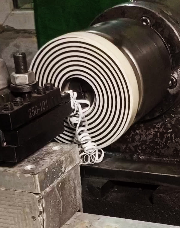
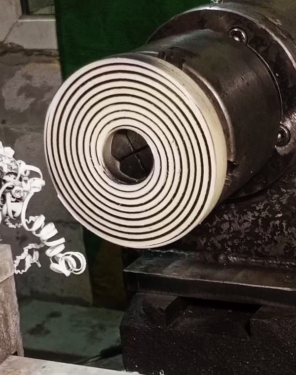
Here is the face spiral cycle cut on my lathe, start to finish (real cut, not an air run). Two frames are attached; a short video of the whole cut (49 s, sped up 2-4x, with music) is on the cycle page:
turngcode.com/en/features/archimedean-spiral/
I painted the face black before cutting so the spiral is easy to see on camera; the paint went on a bit unevenly, so some lands look thinner than they are. The video colour is slightly corrected for contrast, nothing else is edited.
Parameters: diameter 10 -> 110 mm, 3 starts, 2 mm insert (groove) + 2 mm land = 4 mm per turn, spiral lead 12 mm, 1 mm deep in 3 passes + 1 finishing pass, 50 RPM, right-hand.
How it works: the spiral is a G33 move along X, synchronized with the spindle encoder - the same way threads are cut, only across the face instead of along Z. The program works out the lead from the insert width, the land between turns and the number of starts.
Handy detail: the hand of the spiral is set simply by the order of the diameters. Start at the small diameter and finish at the large one - you get a right-hand spiral. Swap the start and end diameters (cut from the outside in) - and the same cycle gives a left-hand spiral, with the same spindle direction.
More on the geometry, lead and speeds, with a sample program:
turngcode.com/en/blog/archimedean-spiral-face-groove/
Questions and criticism welcome.
 And here is the cycle form with exactly these parameters (English UI):
- Geometry: start and end diameter, pitch P (the land between turns), insert width, number of starts, depth, number of passes, finishing allowance and finishing passes, plunge feed.
- Spindle: roughing and finishing RPM.
- Approach / retract: safe X/Z and retract X/Z.
- Options: tool T number in the program, coolant M8, comments, M30 at the end, G7/G8 output.
The program works out the real pitch per turn (insert width + land = 4 mm) and the spiral lead (x 3 starts = 12 mm) by itself. The 2D preview on the right shows the planned G33 path and the current pass, so you can check the spiral before the machine moves. Generate writes the .ngc file, Send to LinuxCNC hands it over to LinuxCNC.
Here is the face spiral cycle cut on my lathe, start to finish (real cut, not an air run). Two frames are attached; a short video of the whole cut (49 s, sped up 2-4x, with music) is on the cycle page:
turngcode.com/en/features/archimedean-spiral/
I painted the face black before cutting so the spiral is easy to see on camera; the paint went on a bit unevenly, so some lands look thinner than they are. The video colour is slightly corrected for contrast, nothing else is edited.
Parameters: diameter 10 -> 110 mm, 3 starts, 2 mm insert (groove) + 2 mm land = 4 mm per turn, spiral lead 12 mm, 1 mm deep in 3 passes + 1 finishing pass, 50 RPM, right-hand.
How it works: the spiral is a G33 move along X, synchronized with the spindle encoder - the same way threads are cut, only across the face instead of along Z. The program works out the lead from the insert width, the land between turns and the number of starts.
Handy detail: the hand of the spiral is set simply by the order of the diameters. Start at the small diameter and finish at the large one - you get a right-hand spiral. Swap the start and end diameters (cut from the outside in) - and the same cycle gives a left-hand spiral, with the same spindle direction.
More on the geometry, lead and speeds, with a sample program:
turngcode.com/en/blog/archimedean-spiral-face-groove/
Questions and criticism welcome.
- Geometry: start and end diameter, pitch P (the land between turns), insert width, number of starts, depth, number of passes, finishing allowance and finishing passes, plunge feed.
- Spindle: roughing and finishing RPM.
- Approach / retract: safe X/Z and retract X/Z.
- Options: tool T number in the program, coolant M8, comments, M30 at the end, G7/G8 output.
The program works out the real pitch per turn (insert width + land = 4 mm) and the spiral lead (x 3 starts = 12 mm) by itself. The 2D preview on the right shows the planned G33 path and the current pass, so you can check the spiral before the machine moves. Generate writes the .ngc file, Send to LinuxCNC hands it over to LinuxCNC.
- scotth
- scotth
03 Oct 2026 17:44
- fmueller
- fmueller
03 Oct 2026 17:20 - 03 Oct 2026 17:32
Replied by fmueller on topic Standalone LinuxCNC machine simulator using the Stepper-Ninja HAL interface
Standalone LinuxCNC machine simulator using the Stepper-Ninja HAL interface
Category: General LinuxCNC Questions
Thanks for testing it and for posting the compiler output.
Your report exposed an incompatibility between the original Stepper-Ninja HAL driver and the new HAL API used by LinuxCNC 2.10. I have now added a compatibility layer that supports both the LinuxCNC 2.9 HAL API and the new 2.10 HAL API.
I released the fix as v0.1.1:
github.com/FredericM88/linuxcnc-sim/releases/tag/v0.1.1
I did not want to publish the fix based on compilation alone, so I also built LinuxCNC 2.10.0~pre2 as a Run-In-Place installation and tested the driver with HAL API 1.
The 2.10 tests included:
- loading and unloading the Stepper-Ninja HAL module
- the expected HAL pins and data types
- bidirectional UDP communication with the simulator
- homing using the simulated inputs
- XYZ motion
- G38.2 probing using the virtual probe input
- persistent material removal, including curved motion
I also added support for building the HAL module directly against a configured LinuxCNC Run-In-Place tree. The build system still supports installed LinuxCNC development files and keeps the source-only compile-check mode.
For an installed LinuxCNC development environment, the compatibility driver can be built with:
The simulator itself and the Stepper-Ninja UDP protocol were not changed for this fix.
If you have a chance to try v0.1.1 on your LinuxCNC 2.10 installation, I would be very interested in whether it now builds and loads correctly there as well. That would also give me an independent 2.10 test outside my development system.
Thanks again for trying the project so quickly and for providing the error log.
Your report exposed an incompatibility between the original Stepper-Ninja HAL driver and the new HAL API used by LinuxCNC 2.10. I have now added a compatibility layer that supports both the LinuxCNC 2.9 HAL API and the new 2.10 HAL API.
I released the fix as v0.1.1:
github.com/FredericM88/linuxcnc-sim/releases/tag/v0.1.1
I did not want to publish the fix based on compilation alone, so I also built LinuxCNC 2.10.0~pre2 as a Run-In-Place installation and tested the driver with HAL API 1.
The 2.10 tests included:
- loading and unloading the Stepper-Ninja HAL module
- the expected HAL pins and data types
- bidirectional UDP communication with the simulator
- homing using the simulated inputs
- XYZ motion
- G38.2 probing using the virtual probe input
- persistent material removal, including curved motion
I also added support for building the HAL module directly against a configured LinuxCNC Run-In-Place tree. The build system still supports installed LinuxCNC development files and keeps the source-only compile-check mode.
For an installed LinuxCNC development environment, the compatibility driver can be built with:
git clone https://github.com/FredericM88/linuxcnc-sim.git
cd linuxcnc-sim
git checkout v0.1.1

git clone https://github.com/atrex66/stepper-ninja.git ../stepper-ninja-hal
git -C ../stepper-ninja-hal checkout --detach eb7e5dfa2e76477e606a47038b07cca5e8a4b424

cmake -S compat/stepper-ninja -B build/compat-hal \
-DSTEPPER_NINJA_SOURCE="$PWD/../stepper-ninja-hal"

cmake --build build/compat-hal -j"$(nproc)"
ctest --test-dir build/compat-hal --output-on-failure

# Result:
build/compat-hal/stepgen-ninja.so
The simulator itself and the Stepper-Ninja UDP protocol were not changed for this fix.
If you have a chance to try v0.1.1 on your LinuxCNC 2.10 installation, I would be very interested in whether it now builds and loads correctly there as well. That would also give me an independent 2.10 test outside my development system.
Thanks again for trying the project so quickly and for providing the error log.
- tuxcnc
- tuxcnc
03 Oct 2026 14:32
Replied by tuxcnc on topic Standalone LinuxCNC machine simulator using the Stepper-Ninja HAL interface
Standalone LinuxCNC machine simulator using the Stepper-Ninja HAL interface
Category: General LinuxCNC Questions
Can't compile ninja hal driver for LinuxCNC 2.10, so your hard work is useless for me.
Building LinuxCNC HAL module stepgen-ninja
/usr/src/stepper-ninja-hal/hal-driver/stepgen-ninja.c:34:13: note: ‘#pragma message: Ethernet version’
   34 |     #pragma message "Ethernet version"
      |             ^~~~~~~
/usr/src/stepper-ninja-hal/hal-driver/stepgen-ninja.c:99:5: error: unknown type name ‘hal_float_t’; did you mean ‘hal_port_t’?
   99 |     hal_float_t *command[stepgens];
      |     ^~~~~~~~~~~
      |     hal_port_t
/usr/src/stepper-ninja-hal/hal-driver/stepgen-ninja.c:100:5: error: unknown type name ‘hal_float_t’; did you mean ‘hal_port_t’?
  100 |     hal_float_t *feedback[stepgens];
      |     ^~~~~~~~~~~
      |     hal_port_t
/usr/src/stepper-ninja-hal/hal-driver/stepgen-ninja.c:101:5: error: unknown type name ‘hal_float_t’; did you mean ‘hal_port_t’?
  101 |     hal_float_t *scale[stepgens];
      |     ^~~~~~~~~~~
      |     hal_port_t
/usr/src/stepper-ninja-hal/hal-driver/stepgen-ninja.c:102:5: error: unknown type name ‘hal_bit_t’; did you mean ‘hal_uint_t’?
  102 |     hal_bit_t *mode[stepgens];
      |     ^~~~~~~~~
      |     hal_uint_t
/usr/src/stepper-ninja-hal/hal-driver/stepgen-ninja.c:103:5: error: unknown type name ‘hal_bit_t’; did you mean ‘hal_uint_t’?
  103 |     hal_bit_t *enable[stepgens];
      |     ^~~~~~~~~
      |     hal_uint_t
/usr/src/stepper-ninja-hal/hal-driver/stepgen-ninja.c:104:5: error: unknown type name ‘hal_u32_t’; did you mean ‘hal_uint_t’?
  104 |     hal_u32_t *pulse_width;
      |     ^~~~~~~~~
      |     hal_uint_t
/usr/src/stepper-ninja-hal/hal-driver/stepgen-ninja.c:107:5: error: unknown type name ‘hal_s32_t’; did you mean ‘hal_sint_t’?
  107 |     hal_s32_t *raw_count[encoders];
      |     ^~~~~~~~~
      |     hal_sint_t
/usr/src/stepper-ninja-hal/hal-driver/stepgen-ninja.c:108:5: error: unknown type name ‘hal_float_t’; did you mean ‘hal_port_t’?
  108 |     hal_float_t *enc_scale[encoders];
      |     ^~~~~~~~~~~
      |     hal_port_t
/usr/src/stepper-ninja-hal/hal-driver/stepgen-ninja.c:109:5: error: unknown type name ‘hal_float_t’; did you mean ‘hal_port_t’?
  109 |     hal_float_t *enc_position[encoders];
      |     ^~~~~~~~~~~
      |     hal_port_t
/usr/src/stepper-ninja-hal/hal-driver/stepgen-ninja.c:110:5: error: unknown type name ‘hal_float_t’; did you mean ‘hal_port_t’?
  110 |     hal_float_t *enc_velocity[encoders];
      |     ^~~~~~~~~~~
      |     hal_port_t
/usr/src/stepper-ninja-hal/hal-driver/stepgen-ninja.c:111:5: error: unknown type name ‘hal_bit_t’; did you mean ‘hal_uint_t’?
  111 |     hal_bit_t *enc_index[encoders];
      |     ^~~~~~~~~
      |     hal_uint_t
/usr/src/stepper-ninja-hal/hal-driver/stepgen-ninja.c:112:5: error: unknown type name ‘hal_bit_t’; did you mean ‘hal_uint_t’?
  112 |     hal_bit_t *enc_reset[encoders];
      |     ^~~~~~~~~
      |     hal_uint_t
/usr/src/stepper-ninja-hal/hal-driver/stepgen-ninja.c:113:5: error: unknown type name ‘hal_float_t’; did you mean ‘hal_port_t’?
  113 |     hal_float_t *enc_rpm[encoders];
      |     ^~~~~~~~~~~
      |     hal_port_t
/usr/src/stepper-ninja-hal/hal-driver/stepgen-ninja.c:131:5: error: unknown type name ‘hal_s32_t’; did you mean ‘hal_sint_t’?
  131 |     hal_s32_t *jitter;
      |     ^~~~~~~~~
      |     hal_sint_t
/usr/src/stepper-ninja-hal/hal-driver/stepgen-ninja.c:132:5: error: unknown type name ‘hal_u32_t’; did you mean ‘hal_uint_t’?
  132 |     hal_u32_t *step_ring_fill;
      |     ^~~~~~~~~
      |     hal_uint_t
/usr/src/stepper-ninja-hal/hal-driver/stepgen-ninja.c:133:5: error: unknown type name ‘hal_bit_t’; did you mean ‘hal_uint_t’?
  133 |     hal_bit_t *step_ring_active;
      |     ^~~~~~~~~
      |     hal_uint_t
/usr/src/stepper-ninja-hal/hal-driver/stepgen-ninja.c:134:5: error: unknown type name ‘hal_bit_t’; did you mean ‘hal_uint_t’?
  134 |     hal_bit_t *step_ring_underflow;
      |     ^~~~~~~~~
      |     hal_uint_t
/usr/src/stepper-ninja-hal/hal-driver/stepgen-ninja.c:135:5: error: unknown type name ‘hal_bit_t’; did you mean ‘hal_uint_t’?
  135 |     hal_bit_t *step_ring_overflow;
      |     ^~~~~~~~~
      |     hal_uint_t
/usr/src/stepper-ninja-hal/hal-driver/stepgen-ninja.c:136:5: error: unknown type name ‘hal_bit_t’; did you mean ‘hal_uint_t’?
  136 |     hal_bit_t *input[96];
      |     ^~~~~~~~~
      |     hal_uint_t
/usr/src/stepper-ninja-hal/hal-driver/stepgen-ninja.c:137:5: error: unknown type name ‘hal_bit_t’; did you mean ‘hal_uint_t’?
  137 |     hal_bit_t *input_not[96];
      |     ^~~~~~~~~
      |     hal_uint_t
/usr/src/stepper-ninja-hal/hal-driver/stepgen-ninja.c:138:5: error: unknown type name ‘hal_bit_t’; did you mean ‘hal_uint_t’?
  138 |     hal_bit_t *rpi_input[32];
      |     ^~~~~~~~~
      |     hal_uint_t
/usr/src/stepper-ninja-hal/hal-driver/stepgen-ninja.c:139:5: error: unknown type name ‘hal_bit_t’; did you mean ‘hal_uint_t’?
  139 |     hal_bit_t *rpi_input_not[32];
      |     ^~~~~~~~~
      |     hal_uint_t
/usr/src/stepper-ninja-hal/hal-driver/stepgen-ninja.c:141:5: error: unknown type name ‘hal_bit_t’; did you mean ‘hal_uint_t’?
  141 |     hal_bit_t *output[64];
      |     ^~~~~~~~~
      |     hal_uint_t
/usr/src/stepper-ninja-hal/hal-driver/stepgen-ninja.c:142:5: error: unknown type name ‘hal_bit_t’; did you mean ‘hal_uint_t’?
  142 |     hal_bit_t *rpi_output[32];
      |     ^~~~~~~~~
      |     hal_uint_t
/usr/src/stepper-ninja-hal/hal-driver/stepgen-ninja.c:157:5: error: unknown type name ‘hal_float_t’; did you mean ‘hal_port_t’?
  157 |     hal_float_t *debug_freq;
      |     ^~~~~~~~~~~
      |     hal_port_t
/usr/src/stepper-ninja-hal/hal-driver/stepgen-ninja.c:158:5: error: unknown type name ‘hal_s32_t’; did you mean ‘hal_sint_t’?
  158 |     hal_s32_t *debug_steps[stepgens];
      |     ^~~~~~~~~
      |     hal_sint_t
/usr/src/stepper-ninja-hal/hal-driver/stepgen-ninja.c:159:5: error: unknown type name ‘hal_bit_t’; did you mean ‘hal_uint_t’?
  159 |     hal_bit_t *debug_steps_reset;
      |     ^~~~~~~~~
      |     hal_uint_t
/usr/src/stepper-ninja-hal/hal-driver/stepgen-ninja.c:161:5: error: unknown type name ‘hal_u32_t’; did you mean ‘hal_uint_t’?
  161 |     hal_u32_t *period;
      |     ^~~~~~~~~
      |     hal_uint_t
/usr/src/stepper-ninja-hal/hal-driver/stepgen-ninja.c:162:5: error: unknown type name ‘hal_bit_t’; did you mean ‘hal_uint_t’?
  162 |     hal_bit_t *connected;
      |     ^~~~~~~~~
      |     hal_uint_t
/usr/src/stepper-ninja-hal/hal-driver/stepgen-ninja.c:163:5: error: unknown type name ‘hal_bit_t’; did you mean ‘hal_uint_t’?
  163 |     hal_bit_t *io_ready_in;
      |     ^~~~~~~~~
      |     hal_uint_t
/usr/src/stepper-ninja-hal/hal-driver/stepgen-ninja.c:164:5: error: unknown type name ‘hal_bit_t’; did you mean ‘hal_uint_t’?
  164 |     hal_bit_t *io_ready_out;
      |     ^~~~~~~~~
      |     hal_uint_t
/usr/src/stepper-ninja-hal/hal-driver/stepgen-ninja.c: In function ‘watchdog_process’:
/usr/src/stepper-ninja-hal/hal-driver/stepgen-ninja.c:367:39: warning: unused parameter ‘period’ [-Wunused-parameter]
  367 | void watchdog_process(void *arg, long period)
      |                                  ~~~~~^~~~~~
In file included from /usr/src/stepper-ninja-hal/hal-driver/stepgen-ninja.c:441:
/usr/src/stepper-ninja-hal/hal-driver/modules/breakoutboard_hal_0.c: In function ‘bb_hal_setup_pins’:
/usr/src/stepper-ninja-hal/hal-driver/modules/breakoutboard_hal_0.c:23:13: error: implicit declaration of function ‘hal_pin_bit_newf’ [-Wimplicit-function-declaration]
   23 |         r = hal_pin_bit_newf(HAL_OUT, &d->input[i], comp_id, name, j);
      |             ^~~~~~~~~~~~~~~~
/usr/src/stepper-ninja-hal/hal-driver/stepgen-ninja.c: In function ‘_receive’:
/usr/src/stepper-ninja-hal/hal-driver/stepgen-ninja.c:445:27: warning: unused parameter ‘arg’ [-Wunused-parameter]
  445 | static int _receive(void *arg)
      |                     ~~~~~~^~~
/usr/src/stepper-ninja-hal/hal-driver/stepgen-ninja.c: In function ‘udp_io_process_recv’:
/usr/src/stepper-ninja-hal/hal-driver/stepgen-ninja.c:480:42: warning: unused parameter ‘period’ [-Wunused-parameter]
  480 | void udp_io_process_recv(void *arg, long period)
      |                                     ~~~~~^~~~~~
/usr/src/stepper-ninja-hal/hal-driver/stepgen-ninja.c: In function ‘udp_io_process_send’:
/usr/src/stepper-ninja-hal/hal-driver/stepgen-ninja.c:630:29: warning: comparison of integer expressions of different signedness: ‘uint32_t’ {aka ‘unsigned int’} and ‘int’ [-Wsign-compare]
  630 |         if (old_pulse_width != *d->pulse_width) {
      |                             ^~
In file included from /usr/src/stepper-ninja-hal/hal-driver/stepgen-ninja.c:49:
/usr/src/stepper-ninja-hal/hal-driver/stepgen-ninja.c: In function ‘rtapi_app_main’:
/usr/src/stepper-ninja-hal/hal-driver/hal_pin_macros.h:65:13: error: implicit declaration of function ‘hal_pin_u32_newf’ [-Wimplicit-function-declaration]
   65 |         r = hal_pin_u32_newf(dir, ptr, comp_id, name, j); \
      |             ^~~~~~~~~~~~~~~~
/usr/src/stepper-ninja-hal/hal-driver/stepgen-ninja.c:882:9: note: in expansion of macro ‘PIN_U32_INIT’
  882 |         PIN_U32_INIT(&hal_data[j].pulse_width, HAL_IN, default_pulse_width, module_name ".%d.stepgen.pulse-width", j);
      |         ^~~~~~~~~~~~
/usr/src/stepper-ninja-hal/hal-driver/hal_pin_macros.h:77:13: error: implicit declaration of function ‘hal_pin_float_newf’ [-Wimplicit-function-declaration]
   77 |         r = hal_pin_float_newf(dir, ptr, comp_id, name, j); \
      |             ^~~~~~~~~~~~~~~~~~
/usr/src/stepper-ninja-hal/hal-driver/stepgen-ninja.c:885:13: note: in expansion of macro ‘PIN_FLOAT’
  885 |             PIN_FLOAT(&hal_data[j].debug_freq, HAL_OUT, module_name ".%d.stepgen.max-freq-khz", j);
      |             ^~~~~~~~~
/usr/src/stepper-ninja-hal/hal-driver/hal_pin_macros.h:31:13: error: implicit declaration of function ‘hal_pin_s32_newf’ [-Wimplicit-function-declaration]
   31 |         r = hal_pin_s32_newf(dir, ptr, comp_id, name, j); \
      |             ^~~~~~~~~~~~~~~~
/usr/src/stepper-ninja-hal/hal-driver/stepgen-ninja.c:890:9: note: in expansion of macro ‘PIN_S32’
  890 |         PIN_S32(&hal_data[j].jitter, HAL_OUT, module_name ".%d.jitter", j);
      |         ^~~~~~~
/usr/src/stepper-ninja-hal/hal-driver/stepgen-ninja.c:980:17: note: ‘#pragma message: Adding export functions. (watchdog)’
  980 |         #pragma message "Adding export functions. (watchdog)"
      |                 ^~~~~~~
/usr/src/stepper-ninja-hal/hal-driver/stepgen-ninja.c:984:13: error: too many arguments to function ‘hal_export_funct’
  984 |         r = hal_export_funct(watchdog_name, watchdog_process, &hal_data[j], 1, 1, comp_id);
      |             ^~~~~~~~~~~~~~~~
In file included from /usr/src/stepper-ninja-hal/hal-driver/stepgen-ninja.c:4:
/usr/include/linuxcnc/hal.h:807:5: note: declared here
  807 | int hal_export_funct(const char *name, void (*funct) (void *, long),
      |     ^~~~~~~~~~~~~~~~
/usr/src/stepper-ninja-hal/hal-driver/stepgen-ninja.c:992:17: note: ‘#pragma message: Adding export functions. (process-send)’
  992 |         #pragma message "Adding export functions. (process-send)"
      |                 ^~~~~~~
/usr/src/stepper-ninja-hal/hal-driver/stepgen-ninja.c:996:13: error: too many arguments to function ‘hal_export_funct’
  996 |         r = hal_export_funct(process_send, udp_io_process_send, &hal_data[j], 1, 1, comp_id);
      |             ^~~~~~~~~~~~~~~~
/usr/include/linuxcnc/hal.h:807:5: note: declared here
  807 | int hal_export_funct(const char *name, void (*funct) (void *, long),
      |     ^~~~~~~~~~~~~~~~
/usr/src/stepper-ninja-hal/hal-driver/stepgen-ninja.c:1004:17: note: ‘#pragma message: Adding export functions. (process-recv)’
 1004 |         #pragma message "Adding export functions. (process-recv)"
      |                 ^~~~~~~
/usr/src/stepper-ninja-hal/hal-driver/stepgen-ninja.c:1008:13: error: too many arguments to function ‘hal_export_funct’
 1008 |         r = hal_export_funct(process_recv, udp_io_process_recv, &hal_data[j], 1, 1, comp_id);
      |             ^~~~~~~~~~~~~~~~
/usr/include/linuxcnc/hal.h:807:5: note: declared here
  807 | int hal_export_funct(const char *name, void (*funct) (void *, long),
      |     ^~~~~~~~~~~~~~~~
/usr/src/stepper-ninja-hal/hal-driver/stepgen-ninja.c: At top level:
/usr/src/stepper-ninja-hal/hal-driver/stepgen-ninja.c:445:12: warning: ‘_receive’ defined but not used [-Wunused-function]
  445 | static int _receive(void *arg)
      |            ^~~~~~~~
/usr/src/stepper-ninja-hal/hal-driver/stepgen-ninja.c:203:17: warning: ‘counter’ defined but not used [-Wunused-variable]
  203 | static uint32_t counter = 0;
      |                 ^~~~~~~
In file included from /usr/src/stepper-ninja-hal/hal-driver/config.h:83,
                 from /usr/src/stepper-ninja-hal/hal-driver/transmission.h:5,
                 from /usr/src/stepper-ninja-hal/hal-driver/stepgen-ninja.c:13:
/usr/src/stepper-ninja-hal/hal-driver/kbmatrix.h:12:14: warning: ‘key_names’ defined but not used [-Wunused-variable]
   12 | static char *key_names[] = {"softkey-00",  // column 0 - row 0
      |              ^~~~~~~~~
gmake[4]: *** [/usr/src/stepper-ninja-hal/hal-driver/build-cmake/stepgen-ninja/Makefile:9: stepgen-ninja.o] Błąd 1
gmake[3]: *** [CMakeFiles/stepgen-ninja.dir/build.make:109: stepgen-ninja/stepgen-ninja.so] Błąd 2
gmake[2]: *** [CMakeFiles/Makefile2:91: CMakeFiles/stepgen-ninja.dir/all] Błąd 2
gmake[1]: *** [CMakeFiles/Makefile2:98: CMakeFiles/stepgen-ninja.dir/rule] Błąd 2
gmake: *** [Makefile:170: stepgen-ninja] Błąd 2
- fmueller
- fmueller
03 Oct 2026 12:54 - 03 Oct 2026 13:27
Standalone LinuxCNC machine simulator using the Stepper-Ninja HAL interface was created by fmueller
Standalone LinuxCNC machine simulator using the Stepper-Ninja HAL interface
Category: General LinuxCNC Questions
Hi,
I've been working on a standalone CNC machine simulator for LinuxCNC and have now published the first experimental version.
The main idea is that the simulator does NOT interpret G-code itself.
LinuxCNC remains responsible for G-code interpretation, trajectory planning, coordinate systems, offsets and compensation. The simulator sits behind LinuxCNC where real motion hardware would normally be connected.
Currently I use the original Stepper-Ninja HAL driver and its UDP protocol as the interface:
The important part of this approach is that the simulator sees the motion that LinuxCNC actually sends to the virtual hardware instead of trying to reproduce LinuxCNC's trajectory planner.
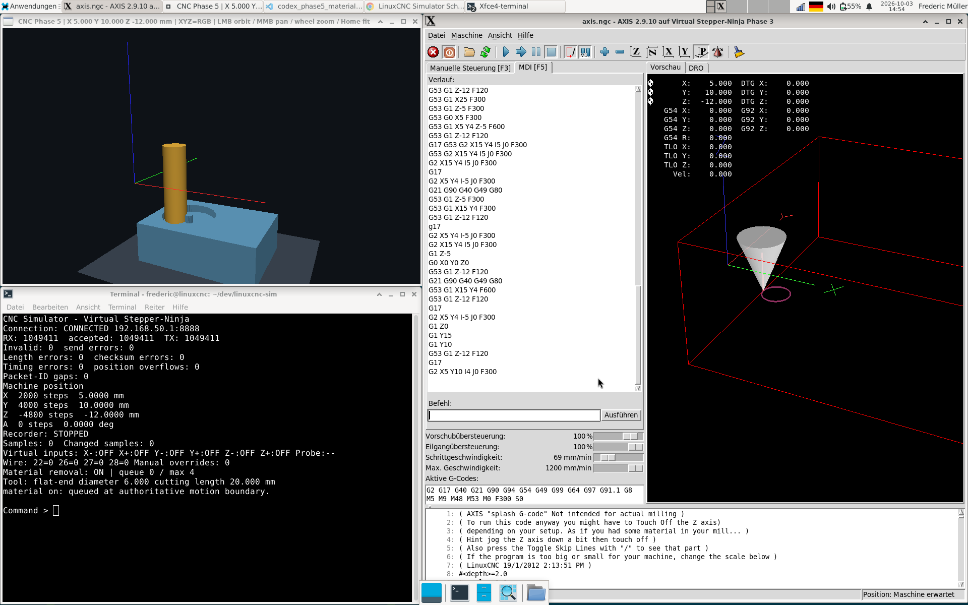
Communication is bidirectional. The simulator can also send virtual machine inputs back to LinuxCNC. I can already use this for limit switches, homing and a simple configurable probe plane.
The current version also contains a sparse voxel workpiece and persistent material removal. Tool movement is processed as continuous swept volumes rather than just removing material at individual sampled positions.
One interesting problem was performance during curved motion. LinuxCNC can generate many small motion segments. Instead of approximating those segments with a larger chord, I batch the actual swept segments for a short time window and calculate the union of their removal volumes. This keeps the resulting voxel state identical while greatly reducing repeated work.
At the moment the simulation is still quite limited:
- flat-end cutter only
- no geometric stock probing yet
- no toolsetter yet
- no spindle/holder model
- no general collision detection
- no rotary material transform
The next area I would like to work on is geometric contact detection. My idea is to use the same contact system later for workpiece probing, a machine-fixed toolsetter and eventually collision detection.
Stepper-Ninja is currently just the interface between LinuxCNC and the simulator. A physical machine does not need to use Stepper-Ninja hardware. I chose it because an existing LinuxCNC HAL driver and a small bidirectional protocol already existed, so I did not have to invent another LinuxCNC hardware interface.
This is my first public release and I consider it experimental development software, not a machine safety system.
Source and v0.1.0:
github.com/FredericM88/linuxcnc-sim
I would be particularly interested in feedback about the architecture. Does placing the simulator behind LinuxCNC at the hardware interface make sense to you? Are there LinuxCNC behaviours or use cases that would be especially useful to test with this approach?
Frederic
I've been working on a standalone CNC machine simulator for LinuxCNC and have now published the first experimental version.
The main idea is that the simulator does NOT interpret G-code itself.
LinuxCNC remains responsible for G-code interpretation, trajectory planning, coordinate systems, offsets and compensation. The simulator sits behind LinuxCNC where real motion hardware would normally be connected.
Currently I use the original Stepper-Ninja HAL driver and its UDP protocol as the interface:
G-code
|
v
LinuxCNC
|
v
Trajectory planner / compensation
|
v
Original Stepper-Ninja HAL driver
|
| UDP
v
linuxcnc-sim
|
+-- virtual machine motion
+-- virtual digital inputs
+-- limit switches
+-- probe input
+-- OpenGL visualization
+-- voxel workpiece
+-- material removal
The important part of this approach is that the simulator sees the motion that LinuxCNC actually sends to the virtual hardware instead of trying to reproduce LinuxCNC's trajectory planner.
Communication is bidirectional. The simulator can also send virtual machine inputs back to LinuxCNC. I can already use this for limit switches, homing and a simple configurable probe plane.
The current version also contains a sparse voxel workpiece and persistent material removal. Tool movement is processed as continuous swept volumes rather than just removing material at individual sampled positions.
One interesting problem was performance during curved motion. LinuxCNC can generate many small motion segments. Instead of approximating those segments with a larger chord, I batch the actual swept segments for a short time window and calculate the union of their removal volumes. This keeps the resulting voxel state identical while greatly reducing repeated work.
At the moment the simulation is still quite limited:
- flat-end cutter only
- no geometric stock probing yet
- no toolsetter yet
- no spindle/holder model
- no general collision detection
- no rotary material transform
The next area I would like to work on is geometric contact detection. My idea is to use the same contact system later for workpiece probing, a machine-fixed toolsetter and eventually collision detection.
Stepper-Ninja is currently just the interface between LinuxCNC and the simulator. A physical machine does not need to use Stepper-Ninja hardware. I chose it because an existing LinuxCNC HAL driver and a small bidirectional protocol already existed, so I did not have to invent another LinuxCNC hardware interface.
This is my first public release and I consider it experimental development software, not a machine safety system.
Source and v0.1.0:
github.com/FredericM88/linuxcnc-sim
I would be particularly interested in feedback about the architecture. Does placing the simulator behind LinuxCNC at the hardware interface make sense to you? Are there LinuxCNC behaviours or use cases that would be especially useful to test with this approach?
Frederic
Time to create page: 0.246 seconds